Chapter 6
So far we’ve talked about very simple models to help us understand how solar cells operate. In the following sections, we’re going to go into more detail, and equip you with some of the same knowledge that solar cell researchers use regularly when they’re testing and evaluating their designs.
Physical Loss Mechanisms
We’ve already talked about a few physical loss mechanisms inside solar cells that designers are trying to overcome, such as charge recombination, and reflections from the front surface. There are other loss mechanisms present, and we’ll be discussing several of those, as well as how they’re usually represented in a circuit model, below.
Series Resistance
In any electric circuit, there is always some energy that is lost as heat as electrons move through a material. This is usually called electrical resistance. The more resistance, the more electrical energy is converted into heat.
The materials and construction of solar cells are similar in the sense that they don’t conduct electricity perfectly. Some of the electrical energy will heat up the material rather than flow through the circuit, and these are called ohmic or resistive losses. Imperfect connections at the front surface contacts are a major source of resistive losses because of the sudden change in material, and difficulty sometimes inherent in bonding to a semiconductor. This resistance is a bigger problem at high current densities, because as we’ve explained before, we have small area wire contacts to minimize recombination at the back surface, and shadowing at the front surface. At higher current densities, we have the problem analogous to a small pipe trying to flow too much water through it, and being the bottleneck for the entire flow.
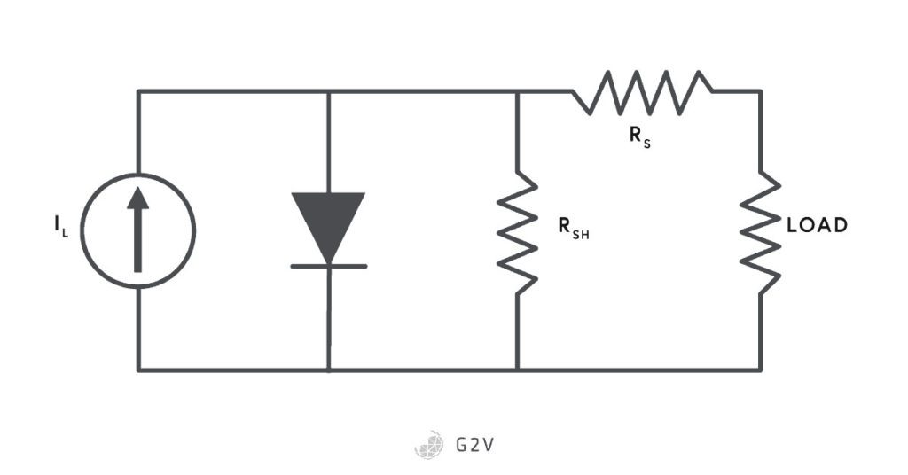
Because this resistance dissipates energy before it gets out of the cell, we can include it in our circuit model as a resistance in series (or inline) with the load, as shown below.
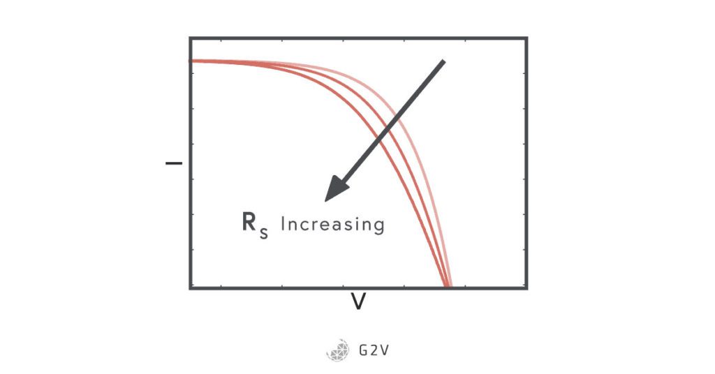
The series resistance has the effect of moving the “cliff” of the diode curve to a lower voltage, as shown below, which ultimately lowers the maximum power we can get out of a solar cell.
Shunt Resistance
The doping of semiconductors into p-type or n-type is never quite perfect, and inevitably there are defects in a given solar cell. These defects can provide alternate paths that electrons can travel through instead of our desired load. When current takes a shortcut to the end instead of going through the desired wire, this is called a short-circuit. Another word for short-circuit is a shunt, so this effect is often represented as a shunt resistance in the circuit model, as shown below. Note that this resistance is connected in parallel with the load, so it is sometimes also called a parallel resistance.
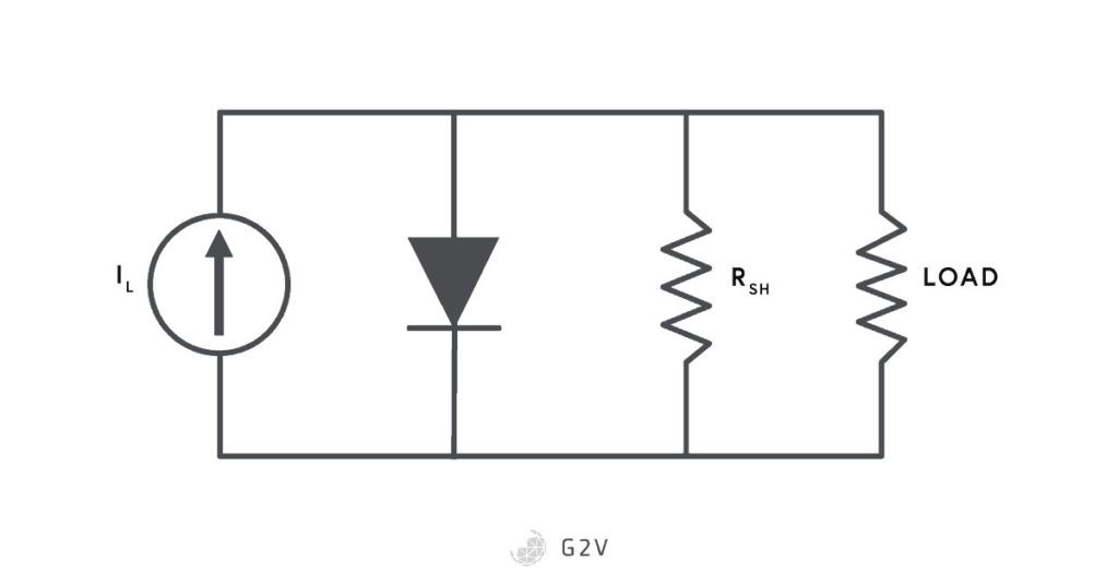
A shunt resistance has the effect of steadily decreasing the current as the voltage is increased (mainly because of Ohm’s Law, V=IR), as shown below. A lower shunt resistance means there are more defects and leakage currents, which reduce the maximum power we can get out of our solar cell.
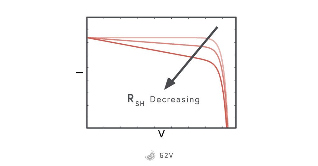
Image Data Source
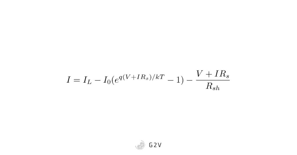
Both of these resistances diminish the effectiveness of the solar cell, so they are called parasitic resistances. Because the effects that are represented by series and shunt resistors are almost always present in solar cells, a more accurate circuit model then includes them both, as shown below.
Making use of Ohm’s Law; that relates voltage, current and resistance (V = IR), we can then update our diode equation to include series and shunt resistances:
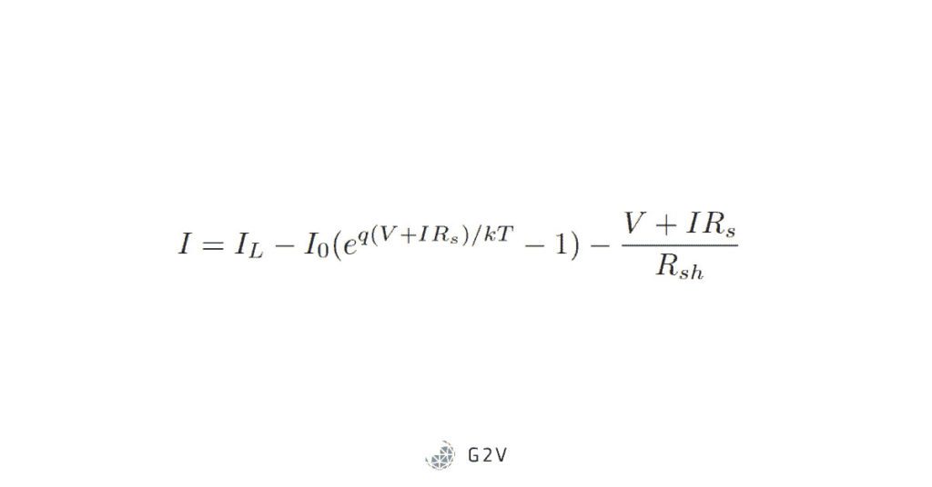
Image Data Source
We’ve just done something quite powerful. We’ve taken some pretty complex physical effects, like charge recombination, and contact resistance, and accounted for them in a mathematical model. Provided we know the values of the series and shunt resistances, we could then use this model to make predictions about device behavior under various conditions. The capability to make predictions, as you might imagine, is huge for researchers, so having models such as this one is very valuable.
There are a few important effects that we still haven’t accounted for in our model, however.
Non-Ideal Diodes
The ideal behaviour described by the Shockley exponential equation is, it turns out, rarely observed. The current through the diode usually has a weaker dependence on voltage (it doesn’t change as quickly). The way this is accounted for in the circuit equation is by introducing a so-called ideality factor n into the exponential, as shown below:
Shockley Exponential Equation
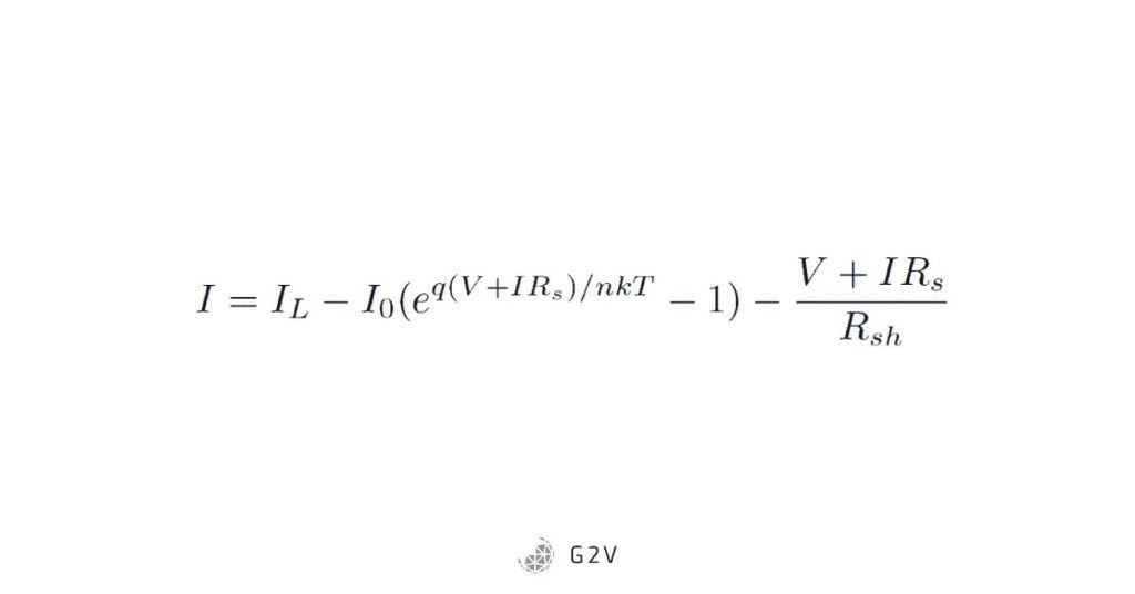
Image Data Source
This ideality factor usually sits somewhere between 1 and 2. It is affected by the relationship between how far a charge carrier will diffuse through the solar cell, compared to the width of the depletion region. If a carrier will usually move past the depletion region, then the diode is behaving ideally. If it doesn’t, then we have to take into account recombination in the depletion region, which results in the ideality factor.
Recombination Diodes
We’ve already talked about charge recombination—this is when the electron-hole pair recombines before the electron has managed to make its way around the circuit and through the load. This recombination, as we described earlier, happens at the edges and surfaces of the device where the charge carriers aren’t under the influence of the junction potential.
The physics driving how quickly and when recombination occurs are fairly complex, but the end result is that the recombination current has an exponential dependence on voltage. Does this sound familiar at all? It’s actually the same as having another diode through which current leaks, so this can be added to our circuit model. The first diode is a result of our solar cell being a semiconductor, whereas the second diode is a result of recombination.
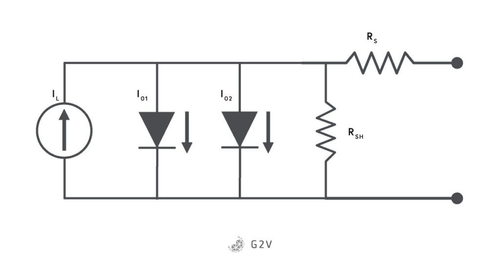
Image Data Source
This diode can be added to our circuit model as another path for current to leak out before reaching our load. The resulting equation is given below, and is an improvement beyond the ideality factor. This is called the two-diode circuit model and is fairly famous because it accounts for a significant number of physical effects while remaining reasonable to depict and understand.
Optical Responsivity
In studying solar cells, researchers want to know, in-depth, exactly how much electricity is generated for a given amount of incident light. They assign values and parameters to represent the proportions at each step of the process. One of the ones we’ve talked about earlier is the overall efficiency number. While this is the best bottom-line, overall value, there are some practical measures that can be used to investigate particular aspects of a solar cell in order to tweak and refine designs. Optical responsivity is one of these.
Optical responsivity is defined as the ratio of the electrical current out compared to the optical power into a solar cell. It’s sometimes also called spectral responsivity. While this might sound similar to overall efficiency, optical responsivity is a function of wavelength. It varies depending on the energy of light shone upon the cell, whereas efficiency is usually given for the entire spectrum of the sun’s radiation (and compares power out rather than current out). A typical graph for optical responsivity of silicon is shown below.
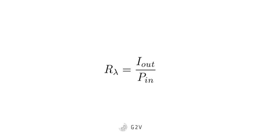
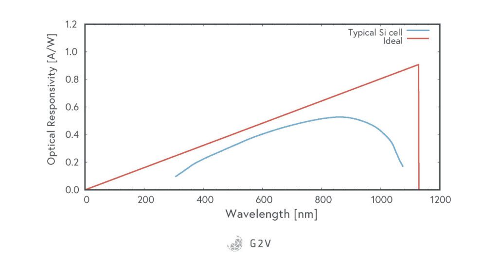
Image Data Source
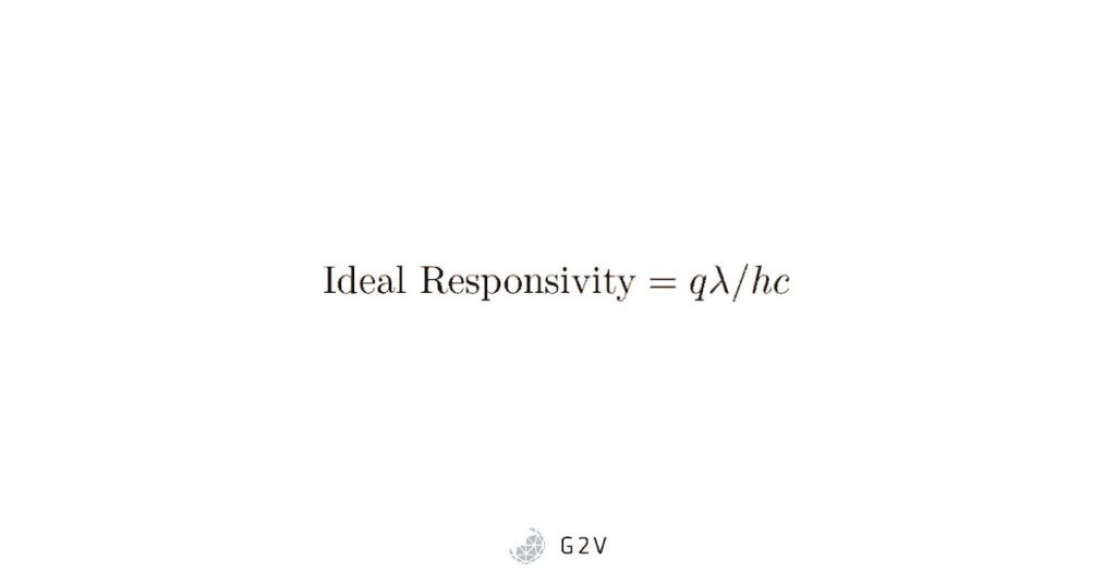
The ideal responsivity, shown above, is where every photon generates an electron. The energy of a photon is given by
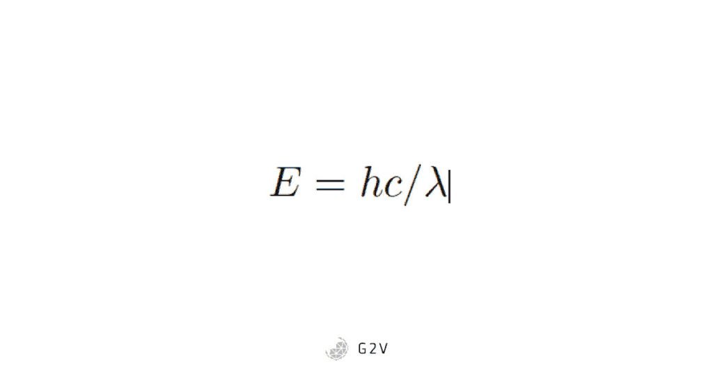
while the charge q of an electron is 1.6×10⁻¹⁹ coulombs. Current is charge per second, while power is energy per second, so in a given second the current divided by the power is just the ratio of these two:
To understand why this curve increases with wavelength, we need to understand that shorter wavelengths have higher energy. That means that shorter wavelengths are dumping much more energy beyond the minimum required by the bandgap. Therefore they’re putting in much more power compared to the electrical current out. A perfect situation is one where the photon energy perfectly matches the bandgap, which occurs at a wavelength of around 1130 nm. However, above this wavelength, the photons no longer have enough energy to bridge the bandgap, so our responsivity plummets to zero.
You’ll notice that a real silicon cell’s optical responsivity actually falls below the ideal curve. This happens for several reasons. The first is that there are losses from reflection as well as photons that don’t create the right lattice vibrations for absorption (remember that silicon has an indirect bandgap). You’ll also remember that there is the unwanted dark current of the photodiode that leaches away some of our ideal output current. The dropoff at higher wavelengths happens because of the bandgap limit, as expected. At shorter wavelengths, the protective glass on the front of the solar cell starts to absorb most of the incoming light.
External Quantum Efficiency (EQE)
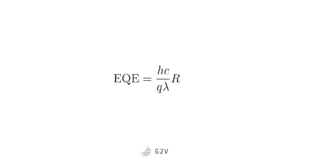
As we mentioned above, the responsivity curve varies across the wavelength spectrum, while generally we’re still only creating a single electron-hole pair for each photon that hits. It’s not telling us the picture of exactly how many electrons we’re getting out per photon, because photon energy is still mixed into the picture. A useful parameter that takes photon energy out of the equation, and instead focuses on how each individual photon is passing through the conversion process, is called quantum efficiency. It’s closely related to responsivity, and can in fact be calculated from it.
Quantum efficiency for a solar cell is defined as the likelihood that an incident photon at a certain energy will deliver an electron to the solar cell’s circuit. You can also think about it as a ratio of charge carriers out compared to photons in. We need to be really specific about which photons we’re talking about, so scientists define two different types of quantum efficiency: internal and external.
Internal Quantum Efficiency (IQE) is the ratio of charge carriers out compared to the photons already absorbed by the cell. This means that the material’s absorptive (or reflective) properties can be ignored. This quantity, therefore, refers more to the solar cell’s ability to move electrons into the external circuit, and how much energy is lost to heat or other means. In other words, it’s concerned about efficiency internal to the solar cell — once the photon is already inside it.
External Quantum Efficiency (EQE) is the ratio of charge carriers out compared to the photons incident on a material. This quantity considers photons moving from the outside world all the way through to electrons in the circuit. The EQE, therefore, is impacted by whether or not a solar cell has an anti-reflective coating. Because we can make measurements external to the cell, and then measure the electrical current out, the EQE is the quantity most commonly used by researchers.
Both the IQE and EQE vary depending on energy, so it is usually represented as a graph of efficiency versus the wavelength of light. An example of an EQE curve is given below.
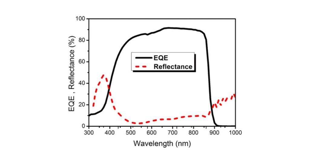
Image Data Source
As we can see in the example graph, the EQE is limited by reflective losses. At higher wavelengths, the photons don’t have enough energy to bridge the band gap, and so the efficiency drops to zero. For lower wavelengths (higher energy), these photons are usually absorbed near the front of the cell, and are therefore close enough to the surface that recombination is a huge factor that drops the efficiency.
The EQE is an important characteristic of a solar cell because it doesn’t depend on the incident spectrum. You’ll notice, for example, that for the most part, the EQE is flat across the wavelength range, which gives us a useful metric for how efficiently photons are being converted into electrons. It is a way to quantify cell design and material quality, and is therefore a parameter every solar cell researcher wants to measure. Before we get into how that’s done, however, we’ll go over how solar cells are tested more generally.