Chapter 3
Semiconductors Basics of a Photovoltaic Solar Cell
As we mentioned, a photovoltaic cell is a semiconductor diode. That might not be a very helpful explanation if you don’t know what a semiconductor is, or what a diode is, so we’ll give you a brief overview here. If you already know, you can feel free to skip ahead to Photovoltaic cell basics.
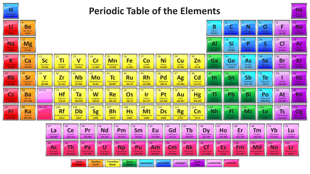
Semiconductors make up microchips, and pretty much anything digital or computerized. To understand what they do differently from other substances, we have to look at the periodic table of elements.
The Right Elements
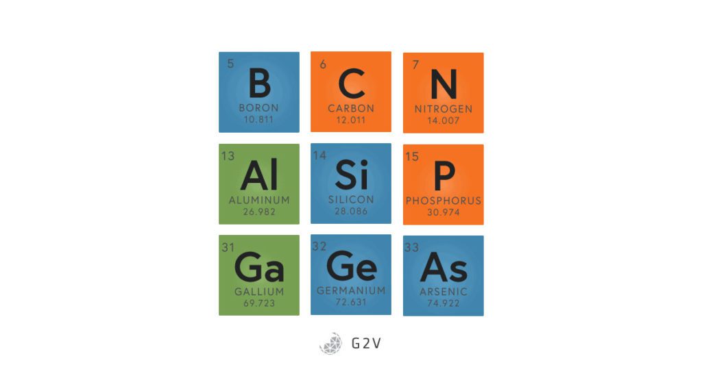
Some of the group III, IV, and V elements of the periodic table.
Carbon (C), silicon (Si) and germanium (Ge) are all in the same column on the periodic table, which means that they all have four electrons in their outer electron shell (or orbital). Most elements “like” to have eight electrons in their outer shell, which makes them more energetically stable (this is called the octet rule). An electron covalent bond is made up of two shared electrons. In order for carbon, silicon and germanium to get their eight electrons, then, they have to form four bonds. This formation of four bonds makes for a great geometry, because four bonding directions create a lattice, or a frame, that forms nice crystals.
Once these elements have their four bonds, the electrons are shared equally, and each atom is content to stay as it is. There are no extra electrons that are free to move around, so there’s no electrical conductivity. For these reasons, these elements (carbon, silicon and germanium) are normally really good insulators when they’re pure. Because silicon is the most common element used within solar cells, we’ll use silicon as an example for the rest of this section.
Exploring N-type Doping and P-type Doping in a Solar Cell
The process of creating a semiconductor starts by taking silicon and making it impure, in a process called doping. This is when you mix silicon with a little bit of another substance, distinguished by two types.
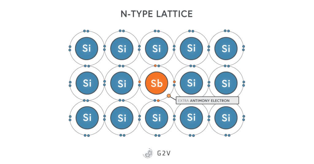
N-type doping (which stands for negative-type doping) is what you get when you mix in a small amount of phosphorus, arsenic, or antimony. You might recognize that these three elements are all situated to the right of silicon on the periodic table, which means they each have five electrons in their outer orbital. When they get put into the silicon lattice, we’re left with an extra electron that is not bonded to anything. It’s free to float around, which means the material can now conduct electricity. Electrons are negative, and since we’re adding an extra electron for every impurity put in, this gives the doping its n-type name.
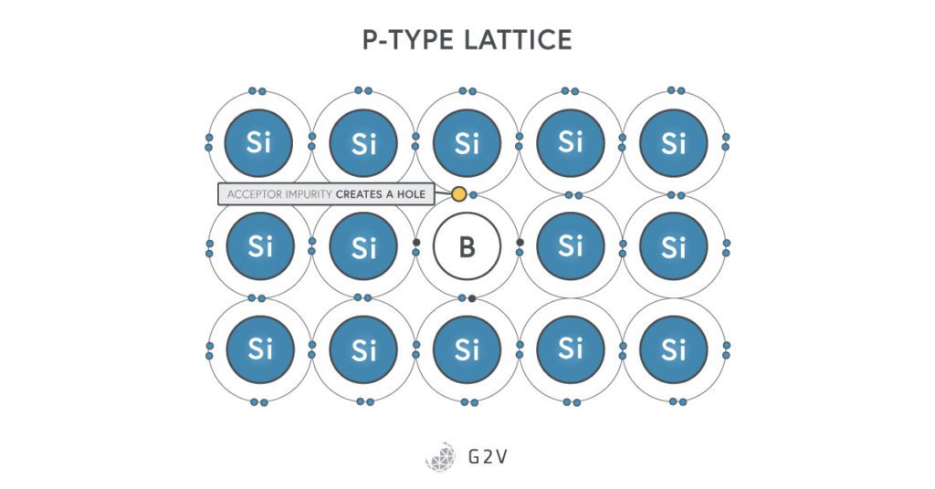
P-type doping (which stands for positive-type doping) is produced when you mix in a small amount of boron or gallium. These elements are to the left of silicon, so they only have three electrons in their outer orbital. When they join into a lattice, there’s one direction that will not have a bond, and will form a “hole” where an electron is missing. This is a place where an electron can jump to, leaving a hole somewhere else. In this way, the hole (or a missing electron) can be thought of as a positive charge that can move around the lattice, which is why this doping is called p-type.
Both the n-type and p-type doping produce materials that can conduct a small amount of electricity. They’re not as good as metal conductors, however, which is why they were given the name semiconductor, meaning partially conductive.
Now that we’ve gained a basic understanding of solar cell theory exploring semiconductors, it’s time to apply this understanding to the most basic semiconductor device: the diode.
Solar Cell Construction
The PN Junction
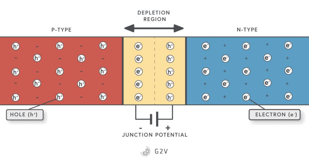
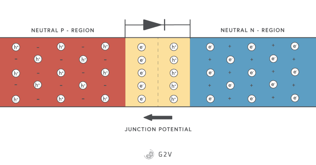
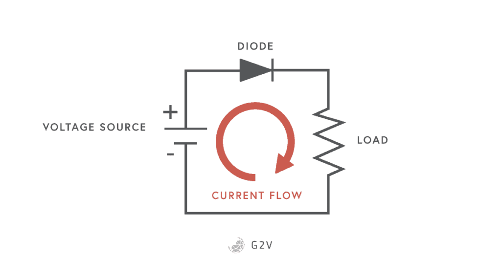
You can make a semiconductor diode by putting an n-type and a p-type semiconductor next to each other. Something pretty interesting happens in the place where the two materials meet, which is called the junction. The side of the p-type semiconductor is called the anode, and the n-type semiconductor is called the cathode.
The Depletion Region
You might have heard the adage that opposites attract, which is true for magnets and electrical charges. This means that the negative electrons in the n-type semiconductor are attracted to the positive charges (vacancies) in the p-type. Some of the electrons move across, and as soon as they leave their parent material, they create a charge difference.
This charge difference results in an electric potential (voltage) that prevents any more charge carriers from moving. We now have a region charges have moved out of; in other words, a layer where there are no more free carriers.
This is called the depletion region because the carriers have been depleted there. No charge can naturally flow across this region so that this semiconductor construction won’t conduct electricity by itself.
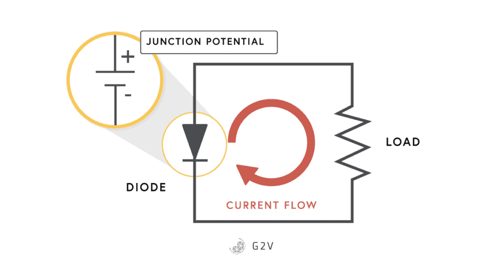
Overcoming the Junction Potential
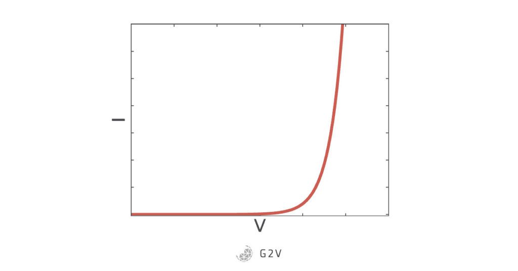
If we hook up a battery or other power source to the diode, we can apply an electric potential (voltage) that overcomes the voltage setup by the semiconductor at the junction. Now charges aren’t stopped, and can move freely once again. Electric current will flow if you apply a sufficient voltage – usually for silicon PN junctions the so-called junction potential needed is about 0.6 V to 0.7 V. The current that flows increases quite quickly once you’ve overcome the junction potential. The IV curve that models this behaviour is shown below, and the solar cell equation above describes the exponential rise and is named after the co-inventor of the transistor, William Shockley.
You can now understand why one of the main things diodes are used for is a one-way gate, because they’ll only conduct current in one direction, and only if the junction potential is overcome.
Now that you understand what a semiconductor diode is, we can go back to our main focus, which is the photovoltaic cell, a specific kind of semiconductor diode.
Photovoltaic Cell Basics
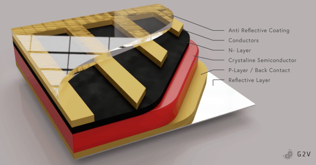
A photovoltaic cell is a diode with a large surface area. The top layer material is kept thin because we want light to be able to pass through it to strike the depletion region. If you remember, the photovoltaic effect happens when light energy is absorbed by an electron.
In the case of a photovoltaic cell, the incident light is absorbed by an electron in the depletion region. It turns out that, for this energy to be captured in a photovoltaic cell, it has to have a certain energy.
What is the Band Gap in Photovoltaics?
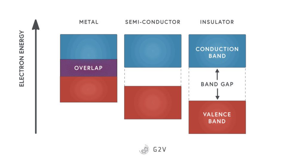
There is a minimum energy that an electron has to obtain before it breaks free of the lattice to move around and conduct electricity. This is the difference between the energy of a bound electron and a free electron.
There’s no one single value, though; there’s actually a range of energies that electrons can have when they’re bound, and this range and state is referred to as the valence band of electrons.
The range of energies and state of electrons that are free to conduct is called the conduction band. The extra energy that electrons have to gain to move from bondage to freedom is the minimum difference between the valence band and the conduction band. We call this difference the band gap.
In silicon, the band gap energy is about 1.11 electron-volts (eV) (an electron volt is the energy that one electron gains when it’s under the influence of one volt of electric potential).
In a semiconductor, the band gap energy is small enough that we can move electrons between being bound and being free, simply by shining light on the material. For comparison, insulators have a band gap energy that is too high (usually greater than 3 eV), meaning that it takes too much energy to free electrons, so under normal conditions, they aren’t conductive. In metals, the valence and conduction bands overlap, so electrons can easily change states between valence and conduction bands, providing a surplus of electrons that can conduct current.
Electron-Hole Pair Generation
All right, now let’s say we have light shining on our semiconductor diode of the right energy—larger than the band gap. It gets absorbed by an electron. This electron moves from the valence band into the conduction band, going from bondage to freedom. It can move around now.
The gap that it left behind is a hole. By shining light on our semiconductor, we’ve created both a conductive electron and a hole. For this reason, the process is often called electron-hole pair generation.
Creating and Capturing The Flow of Electric Current in Solar Cells
Under normal circumstances, the electron-hole pair would quickly recombine because the charges would attract each other. However, the first thing the electron and hole see is the junction potential we talked about earlier in the depletion region. The junction voltage prevents the electron and the hole from recombining right away. In fact, the junction voltage pushes them away from each other, and this is where the science of a photovoltaic cell really shines.
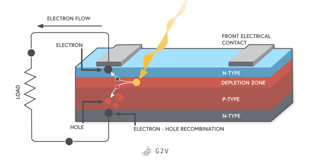
If we connect a wire between the top and bottom of our photovoltaic cell, this electron can now move all the way around through the wire, and reach the hole on the other side of the diode. We’ve just generated a current.
Voilà!
We have our photovoltaic cell: a semiconductor diode that conducts electricity when we shine light on it. We’ve converted energy from the sun into electricity.
Direction of Photocurrent Flow in a Photovoltaics
There are several important details to understand and emphasize here. The first thing is the direction of photocurrent flow. The electric current that flows as a result of light is actually in the opposite direction of the normal diode current. Normally current (defined as the movement of positive charge) moves from the anode to the cathode in a diode. In a photovoltaic cell, however, we see that it’s moving in the opposite direction the long way around: from the cathode to the anode.
Basic (One-Diode) Model of Solar Cells
Remembering that a photovoltaic cell is just a special kind of semiconductor diode, if we want to figure out the total current flowing, we can just add (or in this case, subtract), the diode current from the photoelectric current. If we assume the light shining on a photovoltaic cell stays about the same, then the photoelectric current is just a constant, while the diode current is given by Shockley’s equation. Since the current we’re most interested in for a photovoltaic cell is the photoelectric current, we choose that direction to be positive, resulting in the following solar cell equation for current:
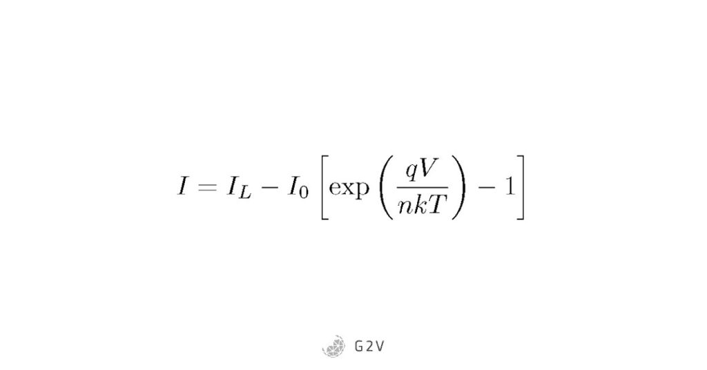
Note that when we don’t have any light shining on the solar cell (IL = 0), the equation is just the Shockley equation. Because this is how the solar cell behaves under dark conditions, the second term in the equation is often called the dark current.
The resulting curve is an inverted and shifted Shockley diode curve that is famous in photovoltaics, called the solar cell IV characteristic curve:
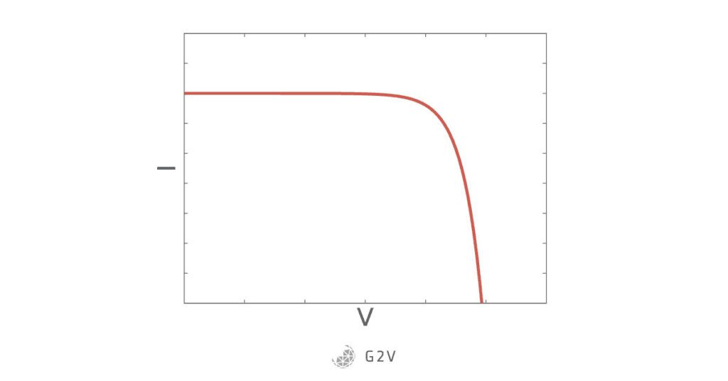
Another quick note is that the way this curve is depicted depends on what is defined as the current-carrying particle. Whether you say that it’s the negative electron, or a positive hole, changes the sign and therefore whether the graph is flipped upside down or not. What’s important is that both definitions are correct ways of representing what’s occurring in a solar cell.
Basic Circuit Model
Another equivalent way to think about the current flow in a photovoltaic cell is that the diode’s natural current flow leeches away some of the current that would normally go to the load.
To better understand the behaviour of the photovoltaic cell, it is common to make use of electric circuit analogies in order to understand what’s physically going on. We call this a circuit model, and we can actually draw the electric circuit associated with the model described above. The photocurrent is then represented by a constant current source connected to a regular diode and our intended load.
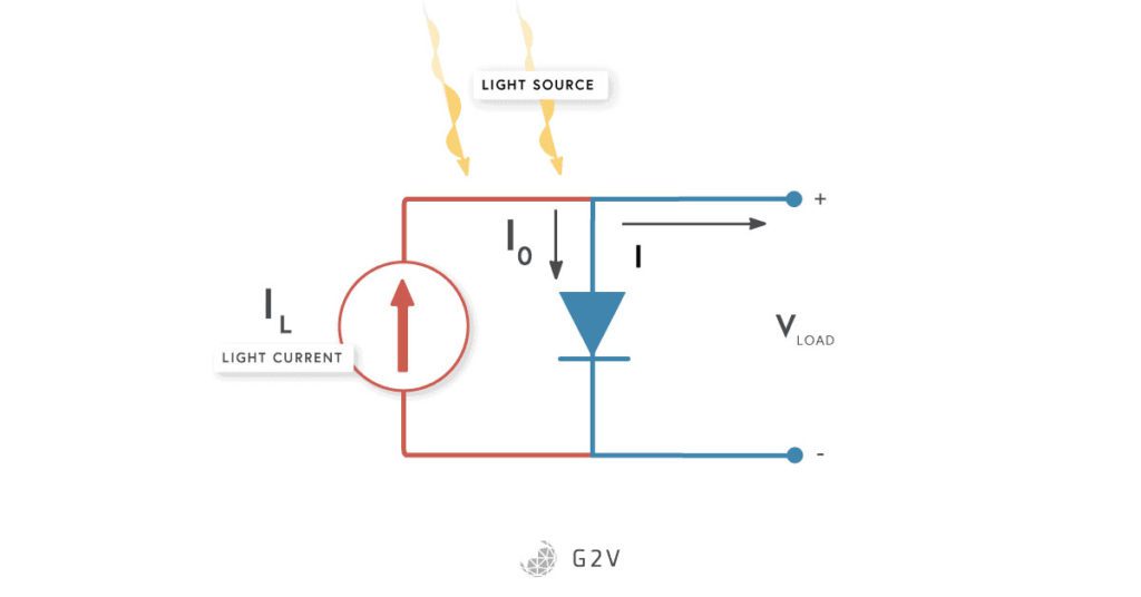
While the model we’ve described doesn’t quite take into account everything that’s happening (as we’ll see later), this is a really good starting point since it benefits from being pretty straightforward to talk about and put measures around. For these reasons, a lot of standards and values have been assigned to describe this IV curve graph and allow solar cell devices to be compared.
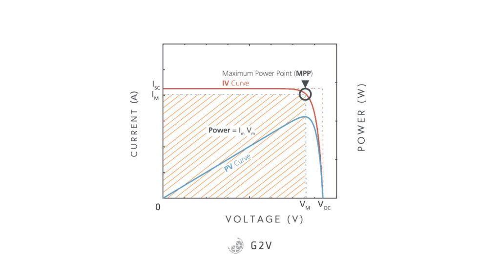
What is the Maximum Power We Can Get?
The maximum current in the device will flow when there’s no resistance; that is, when we hook a simple wire between the terminals. Since this is what happens in a short-circuit, the maximum current is called the short-circuit current, or Isc. This current isn’t doing anything useful, though, and is in fact neutralizing the voltage across the photovoltaic cell.
What we have to do to make the current useful, is to make it do work, or transfer some of its energy into a load. The more load we have, the higher the voltage the cell will have, where all of its junction potential will be used to move the electrons. The highest load we can possibly have is when there’s an infinite amount of resistance, or when the wires aren’t connected at all, and the electrons would have to cross an air gap in order to make it to the other terminal. Because this maximum voltage happens when the circuit is open (i.e. disconnected), we call this the open-circuit voltage, or Voc. In this case, we don’t have a current flowing, so again, we aren’t getting much use of the solar cell. We have to use the solar cell, then, somewhere in between the two extremes of Isc and Voc.
The IV Rectangle
Power in an electric circuit is calculated by multiplying the current by the voltage. Ideally we would have Isc multiplied by Voc. What happens as the voltage in the cell increases, is that the number of electrons actually escaping the depletion region starts to drop. So the curve drops quickly beyond a certain point. However, there is a steady rise of power from the photovoltaic cell as we increase voltage, and before we fall off the “cliff” of the curve. There’s a point where we’ll get the maximum power, and this configuration is called the maximum power point, or MPP.
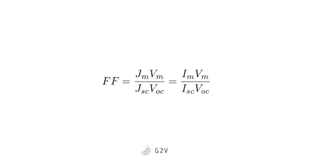
We can see that multiplying current by voltage at the maximum power point (or anywhere else, for that matter) is the same thing as calculating the area of a rectangle on the curve. This rectangle will always be less than the maximum we’d love to achieve if there were a way to get power = Isc x Voc. Because these calculations can be thought of as area calculations, scientists define a term called the Fill Factor (written as FF), that describes how much power we are getting out of the cell compared to the dream of Isc x Voc.
In other words, the Fill Factor represents how close we are to “filling” the rectangle of Isc x Voc.
A quick note worth mentioning is that the current often depends on the area of the solar cell in question. Because researchers build different sizes of solar cells at different stages of development, in order to compare the currents more fairly, the current density is usually used, which is the current divided by the area (usually in units of mA per cm2), symbolized by the letter J. So you’ll often see this symbol in place of the current I that we’ve been talking about so far, as we see in the typical solar cell equation for Fill Factor below.
Source: The Physics of Solar Cells, by Jenny Nelson
All of these metrics are shown below.
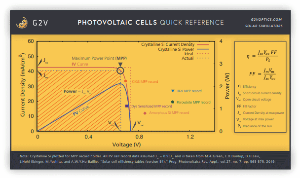
Calculating Solar Cell Efficiency
An important metric of any photovoltaic cell is its efficiency. This is usually defined as the ratio of energy we get out of the cell to the energy put into it by sunlight. We can calculate it using many of the parameters above, by remarking that the input power is the ideal Isc x Voc multiplied by the fill factor. If we know our input power density (or irradiance) of the sun, Ps, we can then calculate solar cell efficiency, which is the division of the two:
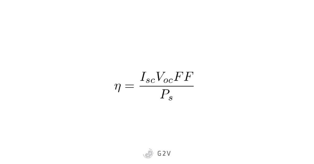
This efficiency (eta above) is one of the most important measurements at the end of the day, because it determines how much electricity humanity can get from solar cells. If we can make photovoltaic cells that convert a greater portion of the sun’s energy, that means we’re that much closer to meeting the energy requirements for a bright future.
Band Gap and Junction Potential Trade-Offs
The last detail to emphasize before we go further is the band gap energy. When we design a photovoltaic cell, we want to make it as easy as possible to generate that electric current, which means having a low band gap energy.
A low band gap energy allows us to absorb more of the sun’s energy (because any light with energy lower than the band gap won’t be absorbed). However, the band gap energy and the junction potential are closely linked. In other words, the lower the band gap energy, the lower the junction potential.
How much energy our freed electron has (i.e. its voltage) is determined by how much it’s accelerated by the junction potential. So if we have a really low band gap energy, we’re going to be generating a really low voltage in our photovoltaic cell. That can be impractical, because for useful electricity, we might then have to chain together a huge number of photovoltaic cells.
– For Advanced Users –
Since these cells are in series, the current through each of the cells is the same. In any set of solar cells, there is a distribution of physical properties that determine solar cell efficiency. As a result, there is a distribution of efficiencies. Under constant illumination, the lowest efficiency will produce the lowest number of charge carriers, limiting current for the entire series of cells.
As you might have already figured out, there’s a balance to be found and some limits to what we can do, which is what scientists and engineers are trying to overcome when they design different types of solar cells.
Get Your Free Photovoltaic Cells Magnet
Fill out the form and we will mail you this magnet for your lab!