
Chapter 4
What Are The Advantages And Disadvantages Of Perovskite Solar Cells?
New technology can have all of the interesting physical behaviours in the world, but if it does not provide any significant benefits it won’t be as widely adopted. In this section, we’ll discuss whether or not the formulations of perovskite semiconductors provide a worthwhile difference to the status quo, as well as what hurdles the technology still has to overcome.
Charge Transport Layers And Junctions: Supporting Materials And Structures Required For Perovskite Solar Cells
So far, our discussion has been focused on the perovskite layer of perovskite solar cells. However, this layer is not the only important part of a solar cell; there are several accompanying components and structures needed for optimal photovoltaic functionality.
These include structures for creating an internal electric field through the intrinsic semiconductor of the perovskite crystal called charge transport layers (CTLs). Beyond that, you also need current collectors from those transport layers out into the circuits where the devices to be powered are connected, whether that is just a single device or the country’s electrical grid. At the most complex end of the spectrum, there are also junction layers for helping to combine multiple specialized layers of perovskites or other photovoltaic materials to create multijunction cells.
Charge transport layers (CTLs) are very important for the operation of current perovskite solar devices. Without them, perovskites can show a significant reduction in PCE.
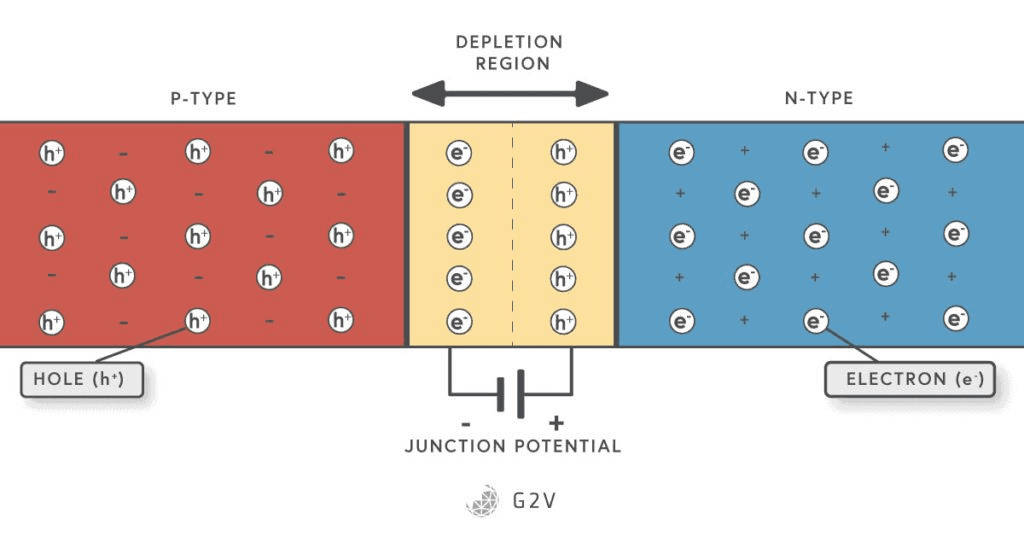
The perovskite absorber layer between the CTLs acts as an uncharged semiconductive material where the incident light can induce charge separation, boosting valence electrons into the conduction band and leaving behind a hole in the valence band, by interacting with the crystal. However, the transport of charges to the respective current collectors is dependent on the electric field, currently created by the charge transport layers (CTLs), just as a silicon cell is dependent on the dopant layers to pull charge carriers out of the depletion zone.
CTLs carry out their transport function by creating favourable junctions with the intrinsic semiconductor of the Perovskite layer. By making it energetically favourable for electrons to enter one CTL and for holes to enter the other, the natural diffusion of free charges from the perovskite into the CTLs creates an intrinsic electric field that helps draw more charges to these layers preferentially. This is similar to how a depletion layer in a traditional pn junction of a silicon solar cell operates.
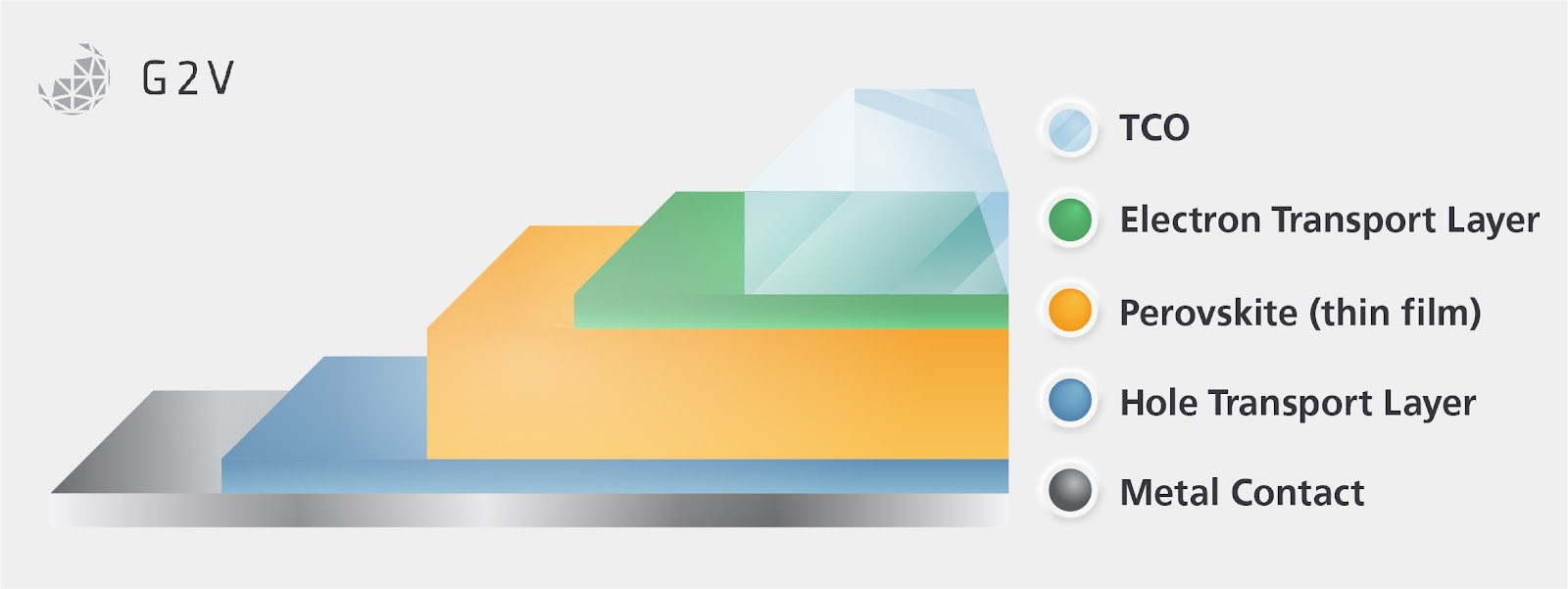
Currently, the most common CTLs are titanium dioxide (TiO2) for the electron transport layer and Spiro-OMe-TAD for the hole transport layer. Alternatives of nickel oxide (NiO) and poly[bis(4-phenyl)(2,4,6-trimethylphenyl)amine] (PTAA), respectively, are also fairly commonly used in those roles.
Thanks to perovskites having high carrier mobility and very thin layers, the application of a hole transport layer (HTL) and an electron transport layer (ETL) is sufficient to generate an electric field throughout the perovskite layer capable of promoting charge transport after electron-hole-pair generation. What order these layers are placed in, relative to the incident light on the solar cell, has some effects on the operation of the device but can be generally considered equivalent for purpose.
Due to the organic and potentially UV-sensitive nature of Spiro-oMeTAD and PTAA, it is more common to find the sunward side of the device to be the ETL, thus defining the orientation of the device as the negative layer (ETL), followed by the intrinsic semiconducting layer (perovskite) and lastly the positive layer (HTL) giving rise to the terminology of “n-i-p construction”.
Although this construction shares the same nomenclature as n-i-p and p-i-n silicon-based semiconductors, there are important differences to note. Perovskite n-i-p and its reverse p-i-n construction is enticing because of the simplicity of the processing stages required to produce them.
By aligning and joining multiple layers without requiring the high energy costs of thermal diffusion or high vacuum of ion implantation doping of a more traditional semiconductor, processing costs can be noticeably reduced.
A downside of this type of construction is the doubling of what are known as “surface defects.”
The interfaces between the different layers are known as surfaces even if they are not necessarily exposed to open air, and the adhesion between the surfaces of the layers is very important to produce a properly functioning solar cell. Poor connections from mismatched crystal orientations, different coefficients of thermal expansion, and/or different electrical conductivities can create forces that delaminate the layers from each other and can prevent the cell from keeping electron-hole pairs separate.
Electron-hole recombination (when the electron-hole pairs are not kept separate) is a key loss mechanism in solar cells that designers seek to minimize as recombination means the charges do not make it out of the device and therefore can’t do any useful work for us.
With a normal p-n junction-based solar cell like silicon, the only surface defects are the contact between the silicon and the electrical contacts at the front and back that complete the circuit. In this aspect, then, silicon-based solar cells have an advantage over perovskites because they have a lower number of surfaces on which defects can form.
Knowing how to manage these surface defects and ensure good electrical conductivity between layers is important for standard perovskite cells but becomes even more so when perovskite technology is used in the fabrication of multijunction cells. While there are many advantages to using perovskites in multijunction cells (which we’ll discuss a bit later), every subjunction that uses perovskites will also be subjected to the same surface defects we’ve been discussing.
Absorption Properties Of Perovskite Structures
If your solar cell has a low absorption and extinction coefficient (i.e. is more transparent to light), then you will require more material to collect incident light before it exits the back of the device.
Solar cell researchers, therefore, want materials with high absorption and high extinction. One of the biggest benefits that Perovskites have is how efficient they are at converting light into excited charge pairs.
Perovskites, as stated earlier, initially started as specialized materials in dye-sensitized solar cells precisely because they were able to absorb light extremely efficiently within very small distances.
In fact, perovskites have an absorption coefficient over 10 times larger than that of silicon, and while the physical scaling is not perfectly 1:1, this higher absorption coefficient means that perovskite solar cells can be approximately ten times thinner than a silicon solar cell to capture the same amount of light.
Such proposed solar cell thickness scaling assumes that the devices have the same quantum efficiency, the ratio between the number of excited charge pairs produced for a specific number of incident photons. Perovskites are known for high quantum efficiencies. This is due to their multiple methods of producing excited charge pairs as stated earlier, but some research is working towards improving that value even further, even over 100% due to some very clever manipulation of the properties of the perovskite crystal structure.
Being able to produce more electrons from the same thickness and number of incident photons gives perovskites an impressive advantage in capability over more traditional materials and designs, not just in terms of output but also in terms of device weight. By having such a high quantum efficiency and high absorption, a perovskite cell has no need to be as thick, and therefore as heavy or rigid, as a traditional solar cell. Even compared to other thin films, perovskites come out ahead because they do not need to sacrifice light collection to get down to smaller form factors.
Another aspect of perovskite solar cell performance closely linked to absorption properties is their good performance at lower light intensities. When the sun is not shining directly on the perovskite solar cell, it is still capable of converting ambient indirect light into usable electricity.
This low-intensity behaviour helps to open up several interesting use cases for the use of perovskite solar cells in interior spaces to power or extend the battery life of small items (such as wearables or other low-power devices).
What Impacts Do Bulk And Surface Defects In Perovskite PV Cells Have On Performance?
Quantum efficiency does not directly translate into power conversion efficiency, though. The excited charges still have to be collected and used in the final circuit. For that to happen, the positive and negative charges must be separated and drawn into their respective transport layers. Preventing that from happening perfectly, however, are the various types of defects within the perovskite crystal.
Defects are any deviation from a perfect crystal in the desired stoichiometric ratio or geometric pattern. They come in many forms and when not controlled they can be very detrimental to the operation of any device, not just semiconductors. Broadly they can be separated into two classifications, bulk defects and surface defects.
Bulk defects are errors within a single crystal such as missing atoms, extra atoms, impurities, atoms in the wrong spot, and so on. These types of defects are simple outcomes of being unable to create a crystal perfectly atom by atom.
Some bulk defects are necessary for certain properties to occur. For example, earlier it was mentioned that ion transport is a method for how charges can be shuttled around inside the crystal. If every position for every mobile ion was perfectly filled within a perovskite crystal, the amount of energy required to move ions would be vastly increased since any incoming ion has to first knock out the atom already occupying the space. Compare this required energy to the energy needed to shift an ion into an already empty space, and you can appreciate the magnitude of the drop in ion mobility that a perfect lattice can cause.
Even if some defects are necessary, all defects impact how current flows through the material. It doesn’t matter if the defect is a missing atom, an extra or several extra atoms, or atoms in the wrong position relative to the rest of the crystal, they all impact the local stress on the crystal and the local electric fields. These alterations act like hills in the path of a bicyclist, either requiring more energy to get over (blocking low voltage charges), or more time spent to get around (increasing the required lifespan of the mobile charge to reach a current collector, so fewer charges make it before recombining, lowering the output current).
The good news about bulk defects in perovskites is that they are not very negatively impactful on the operation of the devices. This insensitivity to bulk defects is theorized to be a combined result of the varied methods of charge separation/transport through the bulk materials, and how the mobility of the X position atoms within the lattice cooperate to allow charges to ignore most of their electronic effects during operation.
By having multiple transport methods you have multiple different interactions with any defects, and by having high mobility of atoms it means that defects are unlikely to stay in one position for very long, giving a statistical equivalence of having the defects “smeared” over a larger volume and having a lower severity of interaction over that volume.
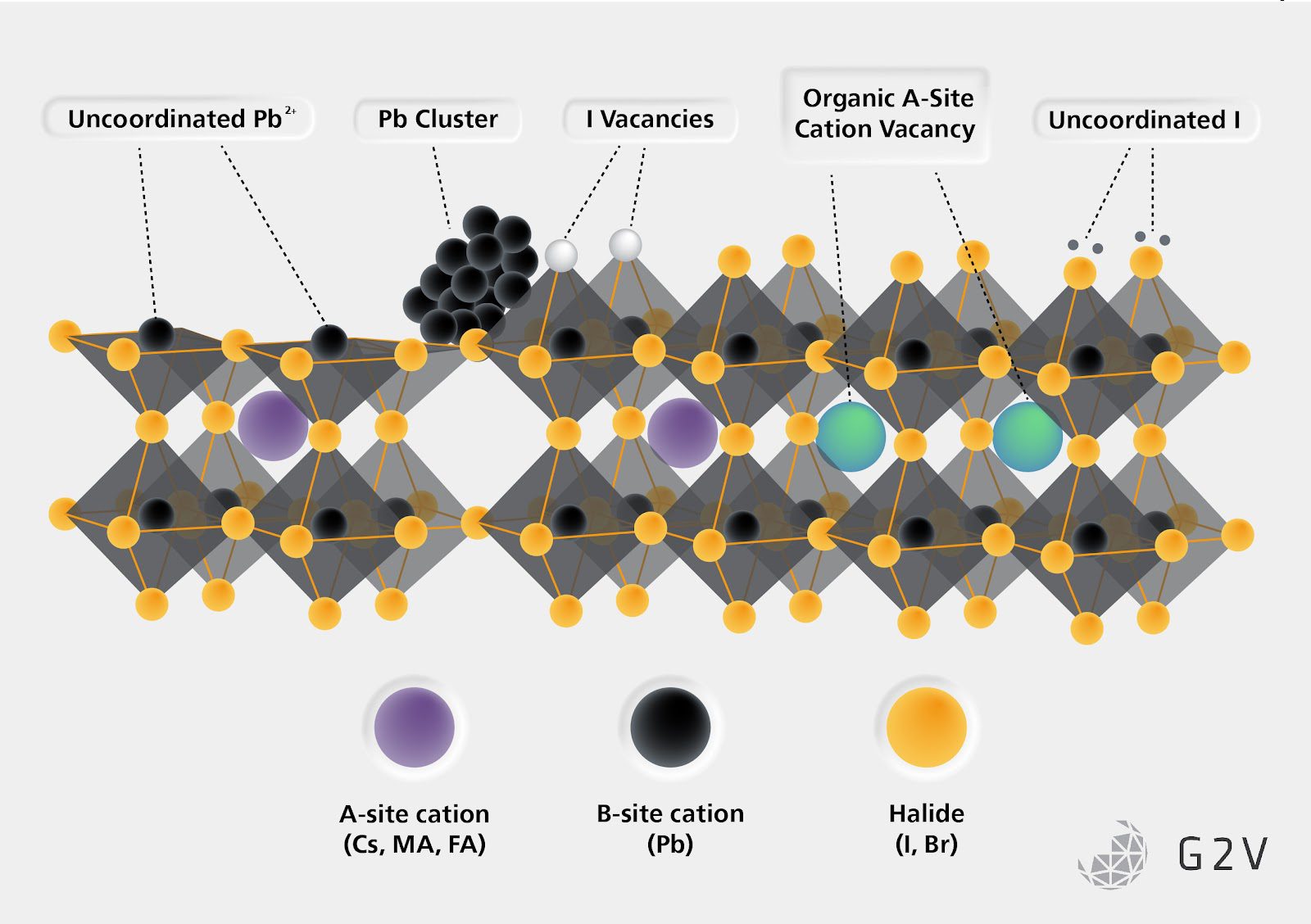
Surface defects, on the other hand, are defects arising from a mismatch in the atomic lattices either between different materials or within the same material type. “Surface” in this case doesn’t refer to actual external surfaces; surface defects are more practically understood as the contact points between two or more lattice-mismatched crystals or materials.
These are the more detrimental types of defects but are also the ones that have more options for reducing their density and impact. A surface defect, such as a crystal lattice mismatch at the interface between a CTL and the perovskite or a grain boundary between two crystal grains within a perovskite, can act as a trap for charges by influencing the local electric field.
Changes in the local internal electric field divert charges from being properly collected and used in the circuit of the solar cell. This is called non-radiative recombination, or surface recombination, as the charges (either holes or electrons) within the defect attract and combine with their opposite charges in the crystal preventing the charge from making it to the electrode.
While minimizing the density of these defects within devices can improve performance and help prevent the onset of early degradation, the number of combinations and variations possible with perovskite fabrication is both a cause and solution to the problem of surface defects.
The vast array of potential perovskite formulations makes it almost inevitable that a composition and fabrication methodology will provide a solution to the formation of unwanted surface defects, both intrinsic and extrinsic. Whether this is from a formulation improving the self-repair of defects within perovskites, or one that prevents their formation during fabrication is the question.
Environmental Considerations: Lead Toxicity And The Search For Alternatives In Perovskite PV Technologies
The flexibility of perovskite material compositions has been a major focus of any single or multi-junction design, which has resulted in a wide variety of different formulations in the effort to reach the desired goal of an efficient, stable, and inexpensive solar panel.
However, one problem has remained fairly intractable since the beginning of perovskite solar cell research.
Whether the perovskite du jour is the original methylammonium lead triiodide, or a more complex one like (Cex, Fa+1-x)Pb(Iy, Br1-y)3 there is one element that is uncomfortably consistent throughout the majority of published research.
Lead (Pb).
Lead has had a fairly negative public reputation since we stopped using leaded gasoline, and for good reasons. Being a cause of neurological, reproductive, and physical disorders such as memory or learning problems in adults and children, reduced fertility in men, miscarriages or stillbirths in women, along with general mood disorders, and digestive issues, it feels only reasonable to be wary of lead or similar heavy metals being allowed to enter the environment from any source.
Unfortunately, lead’s use has persisted in perovskite research due to some of its fundamental atomic characteristics. Perovskites require elements with a specific electron coordination number in the B position of the ABX3 structure to maintain the octahedra of halides. Due to the size of most of the organic molecules used in the A positions, having a large B component is beneficial to make sure there is enough room in the crystal for the A components. Lead appears to be the best choice for meeting the requirements of large ionic size and a coordination number of six.
Lead is still considered by most researchers to be a necessary component for high-efficiency perovskite solar PV. As such the best option is finding methods to prevent the lead from having a method of entering the environment in the first place via proper encapsulation of the solar cells. Ensuring good encapsulation is a good general approach for any future solar cell technology intended for large-scale deployment.
Once solar cell encapsulation is achieved, another key requirement for safe and reliable deployment is implementing methods to capture any lead that might get released should the cell or panel get damaged enough to breach the encapsulation. Such considerations will benefit any large deployment of solar cell technology by increasing a solar cell’s lifetime, and may sufficiently mitigate the risks and concerns associated with lead use in perovskites.
However, as we noted above in the ‘Composition And Common Materials Of Perovskite Solar Cells’ table, there are potential alternatives for lead in perovskites: tin and germanium are just two examples.
These elements are in the same column as lead in the periodic table and therefore share the same electron coordination number in their outer shells. Tin even has a similar ionic size to lead. Given these similarities, there is ongoing research investigating the use of these elements to replace lead completely or in part. Some studies have looked at simple replacements with impressive results for stability and efficiency; however, lead remains present to some extent in many of these reports.
Are Perovskite Solar Cells’ Efficiencies Temperature Dependent?
One behavioural aspect of perovskites that needs to be overcome is related to the method of charge transport within the crystal structure. Namely, the movement of polarons as a significant fraction of current conduction leaves perovskite cells vulnerable to fluctuations in temperature. The “effective mass” is higher than the actual charge it forms around.
This increased effective mass means that the energy required to move this charge through the crystal is higher than for a normal charge in the conduction band. But since polarons are also electrically responsive due to being formed by a free charge becoming coupled to the lattice, local electric fields also play a role in their motion.
Research into the influence of these factors shows that at standard temps (~300K), the strength of the local electric field is a far larger influence on the motion of polarons than temperature if the electric field is strong. Interestingly, at standard temperatures with a weak electric field, thermal motions are more likely to act as a damping force preventing the motion of polarons in any direction.
This electrical field-differentiated change in the effect of temperature on the conductivity of polarons and the final PCE of the cell raises a concern. While bulk material defects are not large enough to maintain charges of significant enough size to alter the intrinsic electric field of the device, surface defects can act as charge concentrations and become traps for free charges (especially polarons). The reason is that surface defects can create local fields noticeably stronger than the internal field of the intrinsic perovskite layer, thus attracting polarons and preventing them from reaching their charge’s respective CTLs. This sort of non-emissive recombination is theorized to be a major component of the known reduction in PCE for perovskites at higher temperatures.
Fortunately, experiments have also shown that the stabilization of perovskite solar cells against temperature fluctuations have a path forward. The replacement/doping of some of the A components in the perovskite structure of organic halide perovskites with inorganic Cs or Rb is showing promising results in stabilization over larger temperature ranges with only minor reductions in overall PCE.
What Is The Radiation Tolerance Of Perovskite Materials For Space-Based Solar Applications?
Due to their thinness, lightweight, and potential for very high PCE, perovskite photovoltaic technologies are attractive for use in space-based applications, an environment where the transportation of every gram is an expensive proposition.
However, for perovskites to have any chance of succeeding in space, there is a unique consideration that needs to be investigated, namely how well these devices handle exposure to high-energy charged particle radiation.
Initial investigations have given positive results. The inherent mobility of a perovskite’s X components allows for the quick replacement of any atoms that are knocked out of position by incoming radiation. The thinness of the devices prevents incoming high-energy radiation from interacting with the panel simply due to them passing through it with minimal interaction.
Finally, the relatively large size but low mass of the A components combined with the general low density of the entire structure mean that when there are interactions they tend to be purely kinetic (rather than chemical or nuclear) creating new bulk crystal defects which, as mentioned earlier, are not especially detrimental to the operation of a PSC.
Perovskite researchers finally utilize the benefits and overcome the concerns about perovskites, improving the capability of single-layer perovskites is important not only for single-junction perovskite solar cells but also for the construction of multijunction cells where both the difficulties and rewards are higher.
Next Chapter 5: Multi-Junctions, Tandem Cells, And Efficiency-Specific Structures For High-Performance Solar Cells
Looking for a cheat sheet with all of the key concepts in this article? Check out the one-page infographic below.
Advantages And Disadvantages Of Perovskite Solar Cells Infographic:
