
Chapter 3
What Are The Limits Of Efficiency For Perovskite Solar Cells?
Once a cell or panel is validated, there is a large array of information available to reference. However, regardless of the different considerations of what is important to different interested parties, one data point spoken of more frequently than any other property of solar technology is Power Conversion Efficiency (PCE). In fact, PCE is spoken of so frequently that it is commonly just called efficiency.
Given that with higher efficiency, a solar panel can generate more power from the same area and create less heat at the same time, it is perfectly understandable that the focus of the most publicly discussed solar research is to find out how to improve the efficiency of any solar cell technology. It’s worth noting,, that, like every other produced good on the international market, additional commercial, bureaucratic and political factors can impact solar cell feasibility and deployment cost. Nevertheless, efficiency remains of key interest.
Perovskites have captured the imagination of both researchers and the public since their debut due to their rapid growth in efficiency. While the rapid rise of perovskite solar cell efficiency to near parity with crystalline silicon is astounding, perovskites still have to contend with the same limitations as previous generation solar technologies such as dye-sensitized solar cells (DSSCs) or CdTe thin-films.
The Shockley-Queisser limit, for example, is still very much in force for perovskites. While perovskites have some advantages over silicon, such as their variable chemistry that allows for the perovskite band gap to be tuned toward a slightly higher single-junction efficiency, in practice this increase is marginal. In the grand scheme, the difference between a maximum efficiency limit of 34% (for perovskites) and 32% (for silicon) in single-junction cells is not that much.
The laws that govern semiconductor-based solar photovoltaic (PV) technologies are the same for perovskites as they are for all other types of solar cells despite their structural and chemical differences from traditional solar technologies. This is good for us as it means the same tricks that solar PV materials like indium gallium arsenide used to create viable multijunction cells to get around the Shockley-Queisser Limit work just as well for perovskite devices.
How Do Perovskite Materials Make Electricity In A Solar Cell?
Fundamentally all solar cells make electricity in the same way. An incoming photon knocks an electron far enough out of place that it doesn’t immediately fall back in, generating an electron-hole pair. The electron and hole then travel through an electrical circuit to power your fridge, air conditioner, or any other connected electronic device. Alternatively, the energy of the electron-hole pair can be stored in a battery, as shown below.
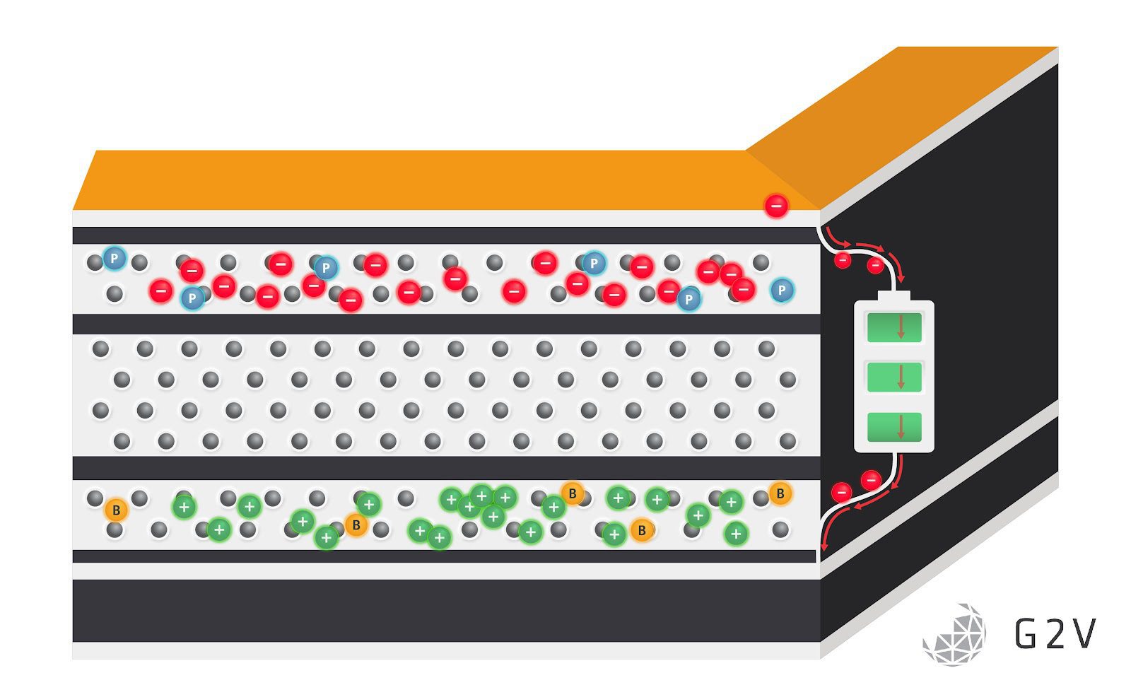
Granted, this is a dramatically oversimplified version of the physics of the photovoltaic effect. However, with the basics firmly in hand, it is easier to explore the important additional details, such as how the band gap of the material defines the amount of energy it takes for that photon to displace the electron. Or how the construction of a thin-film cell bracketed by its electron transport layer (ETL) and hole transport layer (HTL) on either face of the semiconducting layer creates the electric field to move the electron and hole in the desired directions.
Where things get different and interesting, however, is the method the electron uses to get from where it is separated from the hole, and how these two charges travel to where they are collected and used.
Do Perovskite Materials Exhibit Any Unique Physical Transport Mechanics?
Perovskite PV cells are incredibly malleable in their design. As such, they exhibit several unique properties when it comes to their operation and behaviour.
A normal crystalline wafer solar cell is tuned to preferentially conduct charges in certain directions in the crystal relative to whether the charges are positive or negative. This is achieved with carefully controlled doping and the intrinsic electrical field caused by said dopants. Perovskites, meanwhile, show several different methods of charge separation and transport through their atomic lattice: traditional lattice conduction, polaron transport, and ion transport.
Lattice conduction, both electronic and ionic, is the most common method of charge transport. It is simply where charges that are boosted into the conduction bands of the material hop from one location to another in the atomic lattice. Ion transport is related to this as it describes when charged atoms (in an ABX metal halide perovskite, these are normally the X position halides) move through the lattice from defect to defect trying to fill imperfections in the lattice to reduce the energy state of the crystal to as low as possible (ie. a perfect flawless crystal).
Where things get interesting is when a charge is forced into a position where it creates a polaron. A polaron is a structure that arises in strongly dielectric materials that have a free charge attempting to move through the lattice. The electric field of the charge attracts oppositely-charged components of the lattice and repels similarly-charged components. The shifted positions of the neighbours nearest to the charge slightly weaken the neighbour’s electric field strength toward their neighbours, causing the local lattice to flex and stress until the local field is suppressed enough to not impact any more of the lattice.
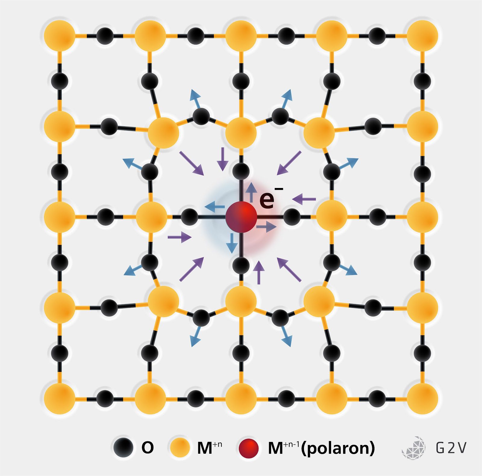
This process creates a kind of pseudo bond between the free charge and the displaced atoms in the local lattice, significantly increasing the effective mass of the free charge as moving it requires altering the pseudo bond length between it and the locally displaced atoms. This means that it takes noticeably more energy to move the charge but that it is also noticeably longer lived than an equivalent charge moving through a lower relative permittivity material like silicon.
With so many physical transport mechanisms at play and with many possible paths to use their properties for better solar cell performance, the question becomes: is the optimization of these transport mechanisms and other perovskite properties worth the effort to explore? Read the next chapter about the advantages and disadvantages of perovskite solar cell technology to explore the answers to this question.
Next Chapter 4: What Are The Advantages And Disadvantages Of Perovskite Solar Cells?
Looking for a cheat sheet with all of the key concepts in this article? Check out the one-page infographic below.
Perovskite Solar Cell Efficiency Infographic:
