Chapter 5
We’ve talked a little about some innovative design solutions that researchers have used to try and optimize solar cells, but the other half of the equation is changing the solar cell material being used. This opens up quite a wide array of options, each with their own advantages and challenges.
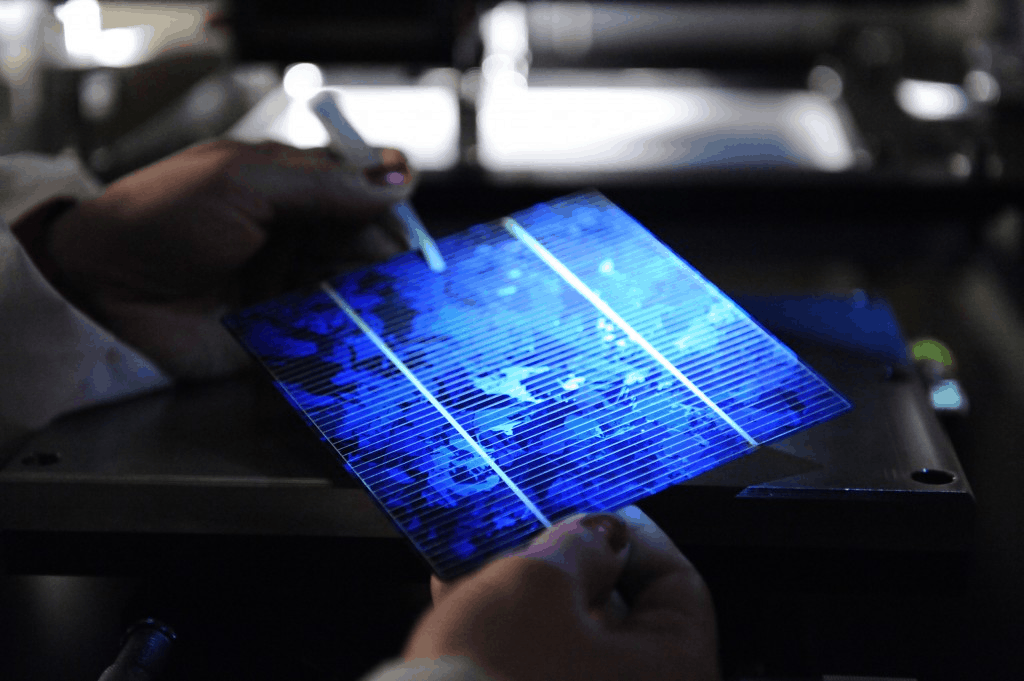
Common Solar Panel Material: Monocrystalline Silicon Solar Cells
Up to this point, all that we have focused on is monocrystalline silicon; that is, silicon made from a single large crystal, with all the crystal planes and lattice aligned. There’s one thing we haven’t yet mentioned about monocrystalline silicon: it has what is called an indirect band gap. This means that, in order for light to be absorbed and send an electron into the conduction band, there has to be a certain change in vibration in the crystal lattice. This specific vibration is not always going to happen, which makes monocrystalline silicon have a low absorption coefficient.
– For Advanced Users –
The specific vibrations we discuss here are phonons – quantized lattice vibrations. Physicists think of these as particles, and when combined with the photon and the electron, we have a three body interaction which are inherently less likely because they have more moving parts that have to be correct to occur.
What’s more is that temperature affects vibrations, which means that how good or bad silicon is at absorbing light is going to be highly dependent on temperature. To get around the low absorption issue, monocrystalline silicon solar cells have to be fairly thick, to give light as much opportunity as possible to be absorbed. We’ve already talked about the other strategies used, such as light trapping and increasing the optical depth.
Silicon, as we can see, is not an ideal material, but we’ve made it work very well. While its band gap energy (1.1 eV) is in the right set of energies for the solar maximum, there’s still some improvement that can be found by choosing a material a higher absorption coefficient and less temperature dependence.
III-V Semiconductor Solar Cells
Semiconductors can be made from alloys that contain equal numbers of atoms from groups III and V of the periodic table, and these are called III-V semiconductors.
Group III elements include those in the column of boron, aluminium, gallium, and indium, all of which have three electrons in their outer shell.
Group V elements include those in the column of nitrogen, phosphorous, arsenic, and antimony, all of which have five electrons in their outer shell.
In a III-V semiconductor, atoms arrange into what’s called a zincblende crystal structure, also known as a face-centered cubic structure or cubic closest packing (CCP).
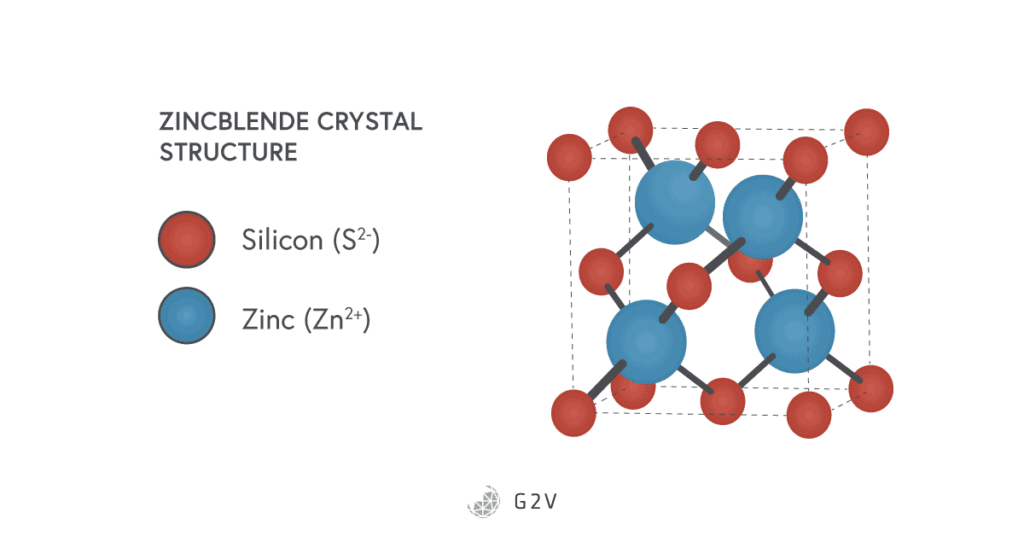
By construction, all the valence electrons in a III-V semiconductor are used up in bonding, so there aren’t any free to conduct. However, by doping in a similar manner to silicon, we introduce impurities that can then make it a semiconductor.
One of the main advantages of III-V semiconductors is that the crystal composition can be varied by replacing some group III atoms with other group III atoms. This changes the bonding and packing distances of the atoms. Why would we want to do this? The reason is that the crystal structure determines the band gap energy. III-V semiconductors, therefore, give us the ability to tune the band gap to our heart’s desire.
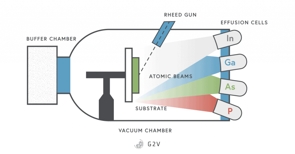
The methods by which III-V semiconductors are made include liquid phase epitaxy (LPE), molecular beam epitaxy (MBE), metal organic chemical vapour deposition (MOCVD), and metal organic vapour phase epitaxy (MOVPE), all of which allow for fine control of the make-up and thickness of semiconductor layers. Unfortunately, these methods are also fairly expensive.
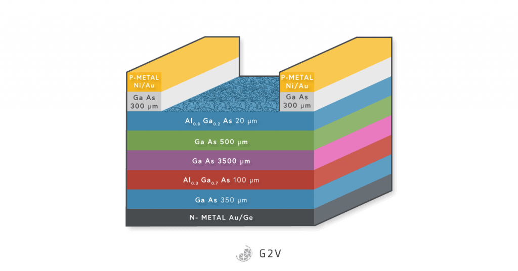
You might have guessed that this freedom to tune the band gap means that III-V semiconductors are what researchers use in developing multi-junction solar cells.
By far the most widely used III-V solar cell is gallium arsenide (GaAs), which has a band gap of 1.42 eV at room temperature. It’s in the range of the ideal bandgaps for solar absorption, and it has the bonus of having a direct-gap absorption, which means that the lattice vibrations don’t matter in deciding whether or not light will get absorbed. That means its absorption coefficient is about ten times better than silicon, and doesn’t have the same temperature dependence.
Other III-V semiconductors include indium phosphide (InP), gallium antimonide (GaSb), aluminium gallium arsenide (AlGaAs), indium gallium phosphide (InGaP), and indium gallium arsenide (InGaAs). In this list we can see how different group III elements are exchanged to make different band gap energies. The exact ratio of one to the other will determine what the final band gap energy will be.
All in all, III-V semiconductors offer a great host of advantages over silicon as a material for photovoltaics. However, the biggest drawback, and one that every new solar technology faces, is cost. The price of silicon is steadily decreasing, and it’s very challenging to compete with that constantly lowering price point, especially when, as in the case of III-V semiconductors, the fabrication methods are so costly.
Nevertheless, there are some situations where III-V semiconductors are the best choice for photovoltaics. Many III-V semiconductors exhibit the property of being radiation hard, which means they don’t degrade as quickly under intense radiation. This makes them ideal for space applications, where the ratio of power to mass is more important (because of the cost to launch it), and where any solar cell will have to survive the intense bombardment of the unfiltered sun’s radiation.

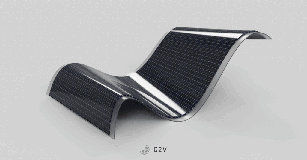
Exploring Thin Film Solar Panel Materials
Monocrystalline silicon and the III-V semiconductor solar cells both have very stringent demands on material quality. To further reduce the cost per watt of energy, researchers sought materials that can be mass-produced relatively easily, and have less stringent demands.
The category of thin film solar cells encompasses a variety of techniques with this goal of mass-production in mind (note that it doesn’t necessarily refer to the thickness of the material itself, since some of the other cells we’ve talked about are also very thin).
In all of these technologies, because of their mass-produced nature, the materials usually have more defects that will prevent the charge carriers from travelling as far as we’d like. To get around or compensate for this issue, materials usually need to be really good light absorbers.
Alternatively, several junctions are used, or the electric potential of the junction is extended to help carriers along, as is done in p-i-n semiconductors which have an intrinsic (undoped) semiconductor layer in the middle.
This solar cell technology produces cells with many defects, making them difficult to dope, and ultimately setting a limit on the junction potential that can be achieved. Defects also make the films more resistive, and overall make the cell’s performance dependent on the density of carriers present. To model this complex behaviour can be very challenging, and this is a topic we’ll tackle in the Data Sets & Models section.
Amorphous Silicon (a-Si)
Probably the best-developed thin-film solar cell technology is amorphous silicon, which means silicon that isn’t arranged into a perfect crystal structure. It’s been in commercial production since 1980, and has the immediate advantage of not needing special crystal vibrations in order to absorb light (since the crystal lattices are all mismatched anyway). Therefore it has a direct band gap, and absorbs more strongly than monocrystalline silicon.
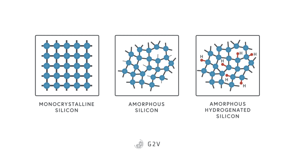
Amorphous silicon does have a problem, because of the mismatched crystal lattices, that some bonds are left dangling. These dangling bonds can interfere with current flow, so often these cells are passivated with hydrogen to latch onto and fill in all the dangling bonds. Although it hasn’t yet achieved the efficiency records of monocrystalline silicon (a-Si currently sits around 10 or 11% efficiency), the less stringent manufacturing methods make amorphous silicon an interesting prospect.
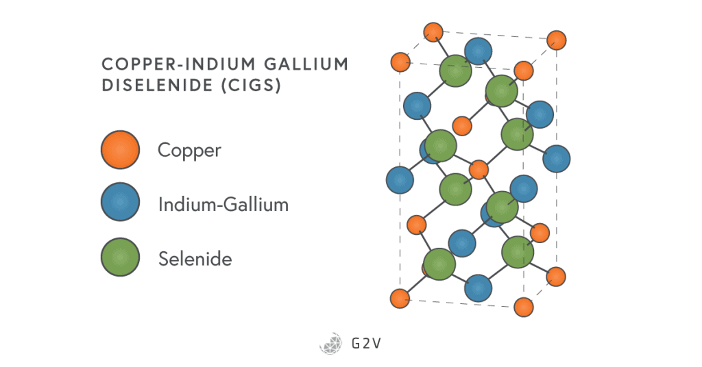
Copper-Indium Gallium Diselenide (CIGS)
It turns out that junctions of CIGS next to CIGS (called homojunctions) don’t have a very high efficiency. A different material is needed for the front, usually cadmium sulfide (CdS), which serves as a window layer to diminish surface recombination.Of all the materials we know, copper-indium diselenide (CIS) has the highest optical absorption.
Its band gap, however, is around 1 eV, so researchers introduced gallium into the lattice to raise the band gap energy closer to the solar ideal. This resulted in the popular copper-indium-gallium diselenide (CuInGaSe2 or CIGS) material for photovoltaic cell construction.
CIGS have what’s called a chalcopyrite crystal structure, shown below. They’re made either by vapour deposition, or by “selenising” copper-indium films.
It turns out that junctions of CIGS next to CIGS (called homojunctions) don’t have a very high efficiency. A different material is needed for the front, usually cadmium sulfide (CdS), which serves as a window layer to diminish surface recombination.
Having a heterojunction introduces many of CIGS’ main challenges, including lattice differences and diffusion of particles between the materials, both of which distort the energy bands throughout the material. The grains of CIGS crystals also limit how far carriers can move before recombining.
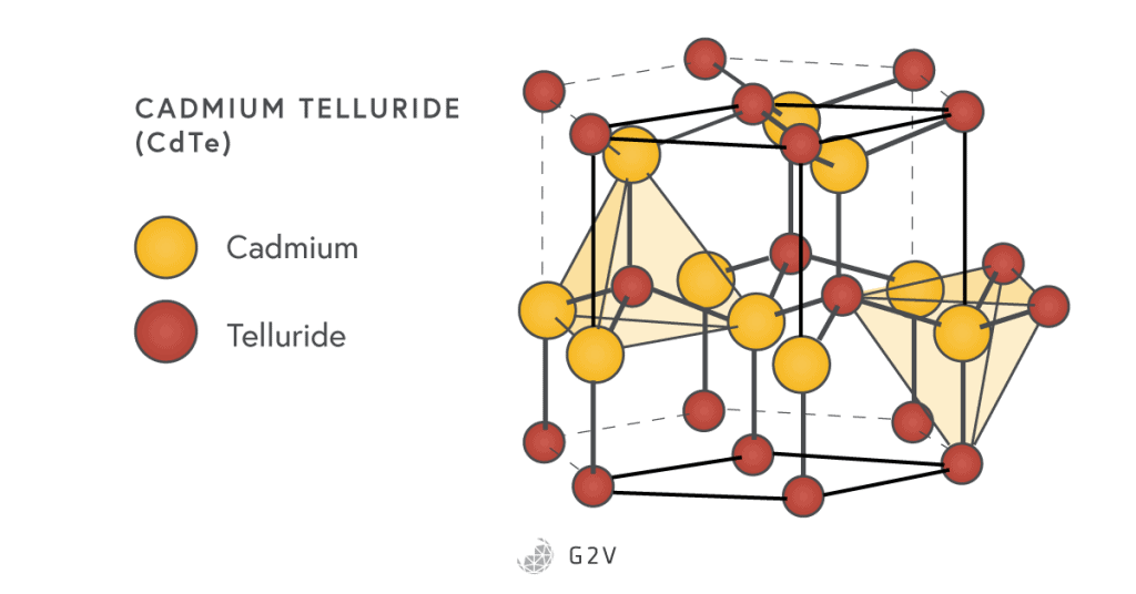
Cadmium Telluride (CdTe)
Cadmium telluride (CdTe) is made from the II-VI group elements, and has a direct band gap of 1.44 eV, making it one of the best-suited materials for photovoltaic applications. It has a wurtzite crystal structure shown below.
However, carriers don’t move through the material as well as they do in GaAs cells, partly because of the higher defect density in CdTe. Higher defects also make CdTe harder to dope, although some treatments have been found to deal with their effects (by saturating the defects’ traps). Heating in Cadmium chloride (CdCl2) was discovered to be crucial in improving the material quality of CdTe cells.
Like CIGS, CdTe also performs better with a CdS heterojunction on the front. The heterojunction introduces the same problems here as in CIGS. The higher density of defects in CdTe at the boundaries results in a high dark-current (the unwanted current that flows when no light is shining on a cell) and a low maximum voltage achievable. Nonetheless, the ideal band gap energy of CdTe is excellent for solar cell applications.
Dye-Sensitized Solar Cells
Solar cells that involve liquid dyes are actually quite similar to batteries. There are electrodes at either end, and a substance that is losing an electron while another is gain an electron (oxidation and reduction, also known as redox). The only difference in a solar cell is that the electron loss (into the conduction band) starts with absorption of a photon.
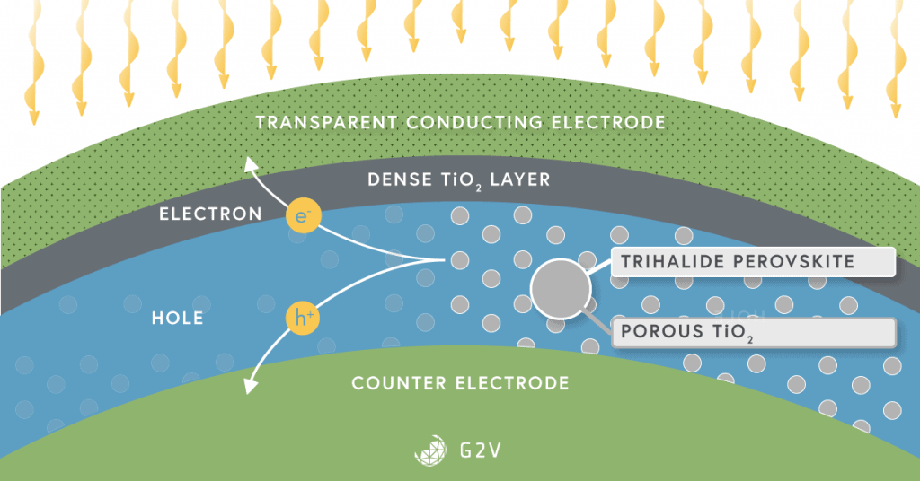
In 1991, Gratzel and Regan realized a low-cost solar cell that used liquid dye on a titanium (IV) oxide film. The overall scheme is shown below, and has come to be known as a general approach of dye-sensitized solar cells.
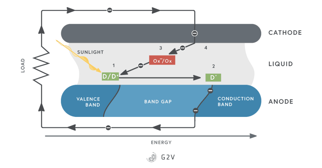
The basic process goes like this: a dye molecule (D) absorbs light and becomes (D*). One of its electrons is now in the conduction band, and moves away from D* (leaving D+). It then moves through the wire from the anode to the cathode. On its way there, it travels through a load and does useful work for us. When it gets to the cathode, it’s absorbed by an oxidizer (Ox) (often iodide). The oxidizer, in turn, replaces the electron needed by D+.
The presence of a liquid, however, made dye-sensitized solar cells not very attractive to researchers, because they could freeze and generally suffered from more instability than other types of solar cells. They also have short transport properties, meaning they don’t respond rapidly enough to capture as much energy as possible. However, they are still being studied and have made great progress, achieving efficiencies as high as about 12%. Some studies that limit the travel distance of carriers are looking very promising as well.
An interesting early application of dye-sensitized solar cells was in sunglasses that could power devices. The lenses were the solar cells.

Finally, dye-sensitized solar cells have also acted as an important stepping stone toward one of the most studied types of solar cells today: perovskites.
Perovskite Solar Cells
A Russian mineralogist named Lev A. Perovski discovered a class of materials that were, some time later in 2009, discovered to be useful in solar cells. Originally they were studied for ferroelectricity and superconductivity. These materials bear his name and are known as perovskites.
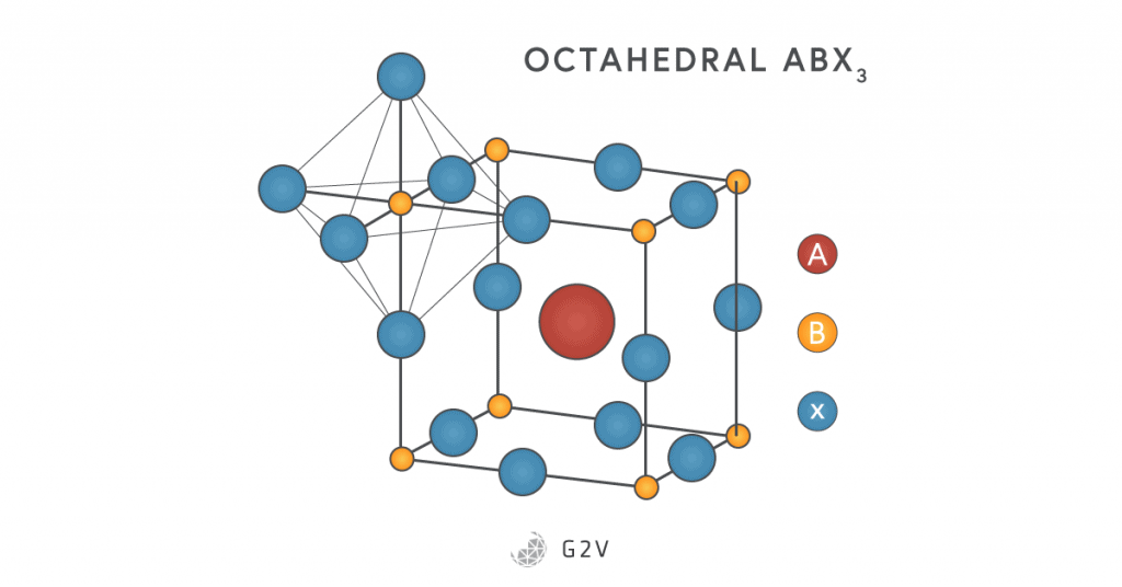
They follow the general formula ABX3, where A and B are both positive ions (cations) located in different parts of an octahedral configuration (where six atoms surround a central one). Usually A is divalent (with 2 electrons in its outer shell), while B is tetravalent (with 4 electrons in its outer shell). X, meanwhile, is a negative ion (anion) that is usually either oxygen or a halogen. The A atom is usually located in the center of a cube of an octahedral crystal near 12 anions, while the B atom is at one of the actual octahedral sites with 6 anions. The diagram shows this unique 3-dimensional structure.
Perovskites, which being ionic dissolve easily in polar solvents, first started as a type of dye-sensitized solar cell, when a methylammonium lead halide perovskite was adsorbed onto titanium (IV) oxide. Like other dye-based solar cells, it exhibited instability and had a fairly low efficiency of 3-4%.
In 2012, however, a long-term stable perovskite solar cell was developed by replacing the liquid electrolyte with a solid hole (p-type) conductor. That led to a marked increase in efficiency and interest in the material which pushed the efficiencies above 20%.

What makes perovskites particularly interesting is that the band gap depends on how flat or two-dimensional the lattice is, so it gives researchers the ability to find the optimal band gap as is done with III-V semiconductors. In contrast to III-V semiconductors, however, perovskites are substantially cheaper. Because of these two combined factors, perovskite technology was selected as one of the biggest scientific breakthroughs of 2013 by the editors of both Science and Nature.

Image Source
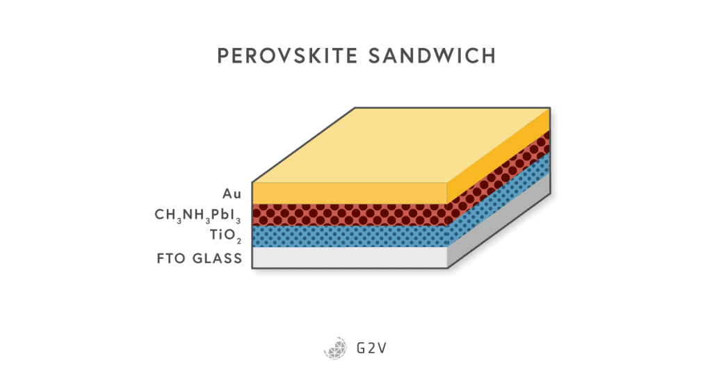
Currently, organo-lead perovskites are at the center of perovskite research. They’ve benefitted from all the research already done in dye-sensitized solar cells, and offer additional advantages of broad spectral absorption, low recombination losses, and the ability to process them in liquid solutions (which is the reason why they’re inexpensive).
An example of a modern perovskite solar cell is shown below.
Organic Solar Cells
Perovskites already use some organic elements (which include carbon, hydrogen, nitrogen and oxygen), but there are other solar cells in development that fall purely on the organic side of the chemistry spectrum. The driving motivation behind organic solar cell development is that the materials would be cheap, as would the production, because mass-producing carbon chains is technology that is well developed in, for example, plastics.
These solar cells have benefited from advances in the development of LEDs based on similar technology, but they still have substantial development ahead in order to be competitive with silicon.
While there are a wide variety of organic solar cell materials, the majority rely on organic molecules with sp2 hybridization – that is, carbon double bonds. The electrons of these double bonds can move to fill in positive charge gaps, which makes the materials hole conductors. Usually they have a band gap around 2 eV, which isn’t ideal for solar absorption.
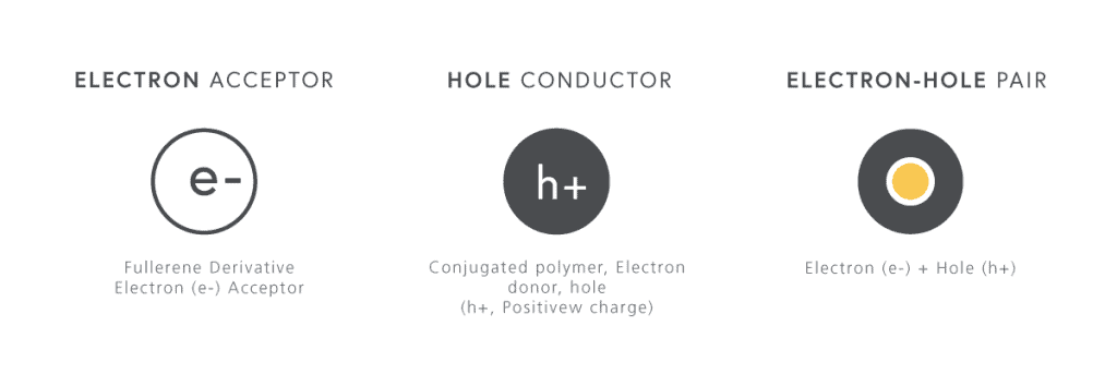
Recently there’s been a lot of focus around organic solar cells using fullerenes, which are a large series of carbon rings attached together in a configuration like a soccer ball (or football).
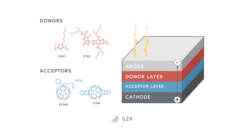
Another challenge faced by organic solar cells is that charge carriers generally don’t travel very far, and the mobility of charge carriers in general is not as strong as it is in traditional semiconductors. They do have a relatively high absorption coefficient, but are still limited to efficiencies between 9-11%.
Graphene Solar Cells
A particular type of organic material used in solar cells is worth discussing because of the particularly high research interest in it: graphene. Graphene is a form of carbon with alternating double-bonds that form a two-dimensional honeycomb sheet.
It was discovered in 2004 by Andre Geim and Konstantin Novoselov at the University of Manchester, who isolated it by peeling a layer off graphite (pencil lead) using scotch tape. They eventually won the Nobel prize for it in 2010.
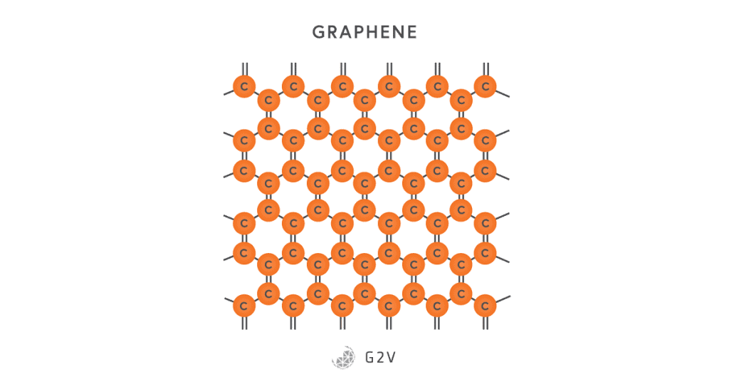
While graphene is stronger than steel and highly conductive (due to the array of double bonds), it has a few other properties that make it particularly useful for solar cells. It is both very flexible and optically transparent (absorbing 2.3% of incident light from UV to IR), making it ideal for application in thin-film solar cells.
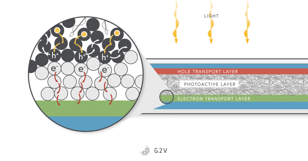
Remember that, in order to capture the current out of the absorption region of a solar cell, we have to run wires from the top to the bottom of the cell, passing through our load on the way. These wires shadow the front surface and decrease the overall light hitting our active area.
Graphene, on the other hand, can be applied as a collector to the front surface, and will serve to transmit much more of the light without shadowing, while still capturing and conducting the charge coming out of the absorption region. Its flexibility allows it to be used in thin-film solar cells, particularly in perovskites, where the main collector used is Indium Titanium Oxide (ITO), a brittle glass that cannot be bent without breaking. Graphene thus unlocks more of the potential benefits of perovskite flexibility.
Graphene has also been used to increase photon collection efficiency in the perovskite active material itself, with some doped graphene allowing larger perovskite grains to form on the carbon network. In this role, it has been used as a carrier transport material.
Finally, it has also been used to protect the unstable perovskite films, because graphene has better physical, chemical, and thermal stability. While graphene by itself doesn’t make a solar cell, in combination with other material properties it unlocks a lot of potential advances.
The Economics of Silicon & the Challenge of Research
As you might have already figured out, photovoltaics is a huge and interesting field of research that, as we’ve said, will play a major role in humanity’s energy future. We also mentioned above that there’s been so much development on monocrystalline silicon solar cells that there’s a steady trend of decreasing price, known as Swanson’s law.
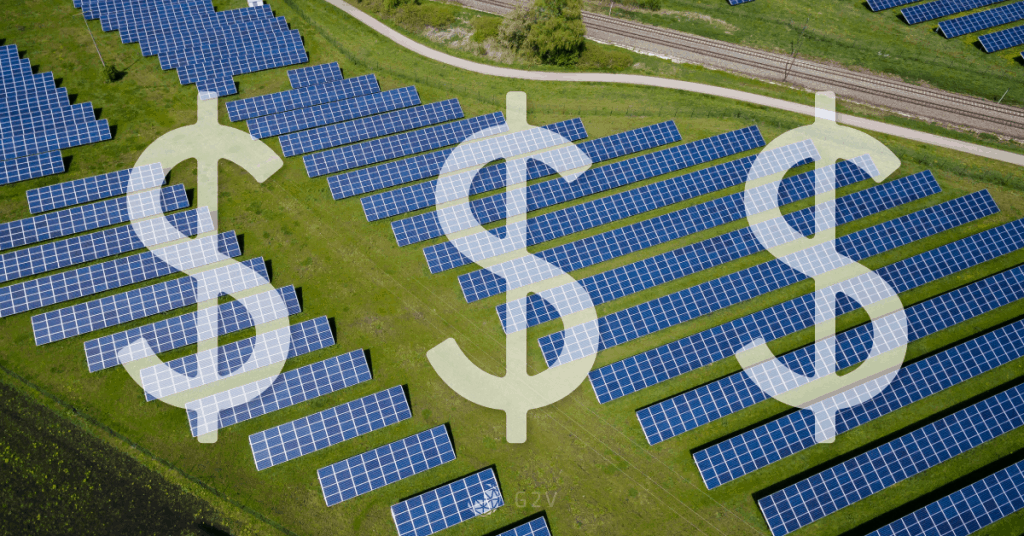
The cost per watt is one of the bottom line metrics in the energy industry. The economies of manufacturing silicon have come very far since the invention of the first solar cell; so far, in fact, that much of the cost is in the installation and accompanying overhead rather than the cost of the devices themselves. The cost per watt for silicon dipped below a US-dollar years ago, and will continue to go down.
Silicon’s dominance in the market can make it very challenging for new photovoltaic technologies to gain traction. Therefore, it’s crucial that researchers get the most accurate data possible, as quickly as possible.