People need energy. This is a simple fact of life, and as society gets more and more complicated and globally interconnected, it only becomes more true. So it is no surprise that there is a constant race to find new ways to produce the energy we need without using all the energy we currently have.
Introduction To Perovskite Solar Cells
If you are interested in clean energy or, more specifically, solar energy, you have probably heard of Perovskite Solar Cells (PSC) technology. Whether you are just learning about them, or are an expert looking for ways to improve test quality and timeline, these chapters should have you covered. We’ll discuss what perovskites are, how they can be used in solar cells, some considerations needed to build a solar cell with perovskites, how they can fail, and how to test and validate them so they won’t.
9 Chapters in this Perovskite Solar Cells Technology Article
Perovskites, like any modern technology, are a complicated topic that can easily overwhelm a person with the amount of available information. To make things easier on you, our reader, we have broken our work into nine easily digestible chapters. Their titles and synopsis are shown below so you can reach what chapter interests you as easily as possible.
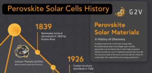 The History and Structure Of Perovskite Solar Cells From an unassuming mineral to a potential replacement for the Multibillion dollar Silicon solar industry. Learn how a certain arrangement of atoms can produce such a wave of optimism. |
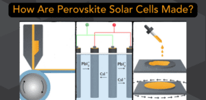 How are Perovskite Solar Cells Made The best research paper is no good unless you can actually make something from it. Learn how many ways perovskites can go from Idea to Item. |
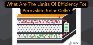 What Are The Limits Of Efficiency For Perovskite Solar Cells? There are limits to everything, and perovskites are no exceptions. But how close are those limits, and are they really as unbreakable as they might seem? |
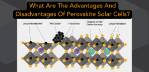 The Advantages And Disadvantages Of Perovskite Solar Cells Perovskites have some definite benefits that excite solar researchers and financiers but also present hurdles that must be addressed. Learn about both sides of the perovskite coin in this chapter. |
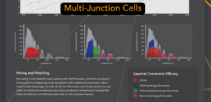 When one just isn’t enough. Stacking layers of cells can give impressive benefits, but also requires overcoming more intricate problems. Can it be viable for perovskites to pursue? |
 The Costs of Perovskites: Sources and Reductions It doesn’t matter if something is better than anything on the market if it is also more expensive than everything on the market. So how do perovskites look to be able to fulfil their promises of being less expensive than current technologies? |
 Energy Efficiency of Perovskite Solar Cells Perovskites are rapidly closing the gap on traditional solar technologies for efficiency. Will they overcome a 40-year headstart or fall prey to the same diminishing returns? |
 Testing And Validating Perovskite Solar Cells With all the optimistic news about perovskites, how do researchers and manufacturers ensure that their devices meet expectations? And how do they convince others that they are? |
 What Applications Exist For Perovskite Solar Cells So once all the proof is in, and solutions for Perovskites’ current problems are found. Where will we see Perovskite solar technologies in our modern life? |
Perovskite Solar Cells Technology Article References
In the course of researching the 9 chapters for this indepth exploration of Perovskite solar cells, from their history, structure, mechanisms, manufacturing, problems, cost, efficiency, and future potential we read hundreds of articles and built our final product on these 118 references. While hyperlinks are provided in the chapters themselves, the full list is provided for you here.
A History of Perovskite Solar Cells. (n.d.). Retrieved September 8, 2022, from https://blog.bccresearch.com/a-history-of-perovskite-solar-cells
Perovskite Materials (Precursors) | Shipped Worldwide | Ossila. (n.d.). Retrieved September 8, 2022, from https://www.ossila.com/en-ca/collections/perovskite-precursor-materials
IEC Standard – Home. (n.d.). Retrieved September 8, 2022, from https://www.iecee.org/dyn/www/f?p=106:49:0::::FSP_STD_ID:61350
Best Research-Cell Efficiency Chart | Photovoltaic Research | NREL. (n.d.). Retrieved September 8, 2022, from https://www.nrel.gov/PV/cell-efficiency.html
Lead poisoning – Symptoms and causes – Mayo Clinic. (n.d.). Retrieved September 27, 2022, from https://www.mayoclinic.org/diseases-conditions/lead-poisoning/symptoms-causes/syc-20354717
News Release: Researchers Improve Safety of Lead-Based Perovskite Solar Cells | News | NREL. (n.d.). Retrieved September 27, 2022, from https://www.nrel.gov/news/press/2020/researchers-improve-safety-lead-based-perovskite-solar-cells.html
Spin Coating: Complete Guide to Theory and Techniques | Ossila. (n.d.). Retrieved October 2, 2022, from https://www.ossila.com/en-ca/pages/spin-coating
An Overview of the Types of Perovskite Solar Cells. (n.d.). Retrieved October 2, 2022, from https://resources.system-analysis.cadence.com/blog/msa2021-an-overview-of-the-types-of-perovskite-solar-cells
crystal defect | Definition, Types, & Facts | Britannica. (n.d.). Retrieved October 2, 2022, from https://www.britannica.com/science/crystal-defect
Accelerated aging test suggests decades-long performance is possible for new perovskite solar cell – The American Ceramic Society. (n.d.). Retrieved October 4, 2022, from https://ceramics.org/ceramic-tech-today/energy-1/accelerated-aging-test-suggests-decades-long-performance-is-possible-for-new-perovskite-solar-cell
What are Surface Defects? – Definition from Corrosionpedia. (n.d.). Retrieved October 4, 2022, from https://www.corrosionpedia.com/definition/1614/surface-defects
Full Record of PV Cell Efficiency Data Now Publicly Available | Photovoltaic Research | NREL. (n.d.). Retrieved October 4, 2022, from https://www.nrel.gov/PV/insights/posts/full-record-of-PV-cell-efficiency-data-now-publicly-available.html
Flash Test: technical background and importance. (n.d.). Retrieved October 5, 2022, from https://sinovoltaics.com/learning-center/testing/flash-test-technical-background-and-importance/
Cite this answer. (n.d.). Retrieved October 6, 2022, from https://www.researchgate.net/post/Charge_transport_in_Perovskite_solar_cell/59ccd6ac48954c2f7850a4f4/citation/download
Cite this answer. (n.d.). Retrieved October 6, 2022, from https://www.researchgate.net/post/How_to_calculate_short_circuit_current_density_Jsc_using_EQE/5f3c18abdda1db61166154ac/citation/download
Slot-Die Coating Theory, Design & Applications | Ossila. (n.d.). Retrieved October 6, 2022, from https://www.ossila.com/en-ca/pages/slot-die-coating-theory
Lev Perovski – Wikipedia. (n.d.). Retrieved October 6, 2022, from https://en.wikipedia.org/wiki/Lev_Perovski
Piezoelectric Materials: Crystal Orientation and Poling Direction | COMSOL Blog. (n.d.). Retrieved October 6, 2022, from https://www.comsol.com/blogs/piezoelectric-materials-crystal-orientation-poling-direction/
Ruddlesden-Popper phase – Wikipedia. (n.d.). Retrieved October 6, 2022, from https://en.wikipedia.org/wiki/Ruddlesden-Popper_phase
Methylammonium lead halide – Wikipedia. (n.d.). Retrieved October 6, 2022, from https://en.wikipedia.org/wiki/Methylammonium_lead_halide
Theory of Solar Cells | G2V Optics Inc. (n.d.). Retrieved October 6, 2022, from https://g2voptics.com/photovoltaics-solar-cells/theory-of-solar-cells/
Types of Photovoltaic Cells | G2V Optics Inc. (n.d.). Retrieved October 6, 2022, from https://g2voptics.com/photovoltaics-solar-cells/types-of-solar-cells/
Shockley–Queisser limit – Wikipedia. (n.d.). Retrieved October 6, 2022, from https://en.wikipedia.org/wiki/Shockley%E2%80%93Queisser_limit
What is Photovoltaics | G2V Optics Inc. (n.d.). Retrieved October 6, 2022, from https://g2voptics.com/photovoltaics-solar-cells/what-is-photovoltaics/
Perovskite Precursor Ink for Air Processing | Ossila. (n.d.). Retrieved October 6, 2022, from https://www.ossila.com/en-ca/products/perovskite-ink-air
Solar Panel Material Polysilicon Is Extending a Price Rally – Bloomberg. (n.d.). Retrieved October 6, 2022, from https://www.bloomberg.com/news/articles/2022-07-06/solar-panel-material-polysilicon-is-extending-a-price-rally
PE15 – Pathways and Challenges of reliability testing for perovskite based photovoltaic devices. (n.d.). Retrieved October 6, 2022, from https://www.wcpec-8.com/index.php/programme-2022?view=article&id=99
Solar Simulation – Sun Simulators: AM0-AM40 | AM1.5G Standards | G2V Optics Inc. (n.d.). Retrieved October 6, 2022, from https://g2voptics.com/solar-simulation/
How Solar Simulators Enhance Aerospace Photovoltaic Testing. (n.d.). Retrieved October 6, 2022, from https://g2voptics.com/aerospace-PV-testing
IEC 60904-9:2020 Standard for Solar Simulators | G2V Optics. (n.d.). Retrieved October 6, 2022, from https://g2voptics.com/iec-60904-9-2020/
What is the Calibrated Output Spectral Irradiance for a Solar Simulator? (n.d.). Retrieved October 6, 2022, from https://g2voptics.com/calibrated-spectral-irradiance/
How To Test Solar Cells | G2V Optics Inc. (n.d.). Retrieved October 6, 2022, from https://g2voptics.com/photovoltaics-solar-cells/solar-cell-testing/
Series Resistance | PVEducation. (n.d.). Retrieved October 6, 2022, from https://www.PVeducation.org/PVcdrom/solar-cell-operation/series-resistance
Fill Factor | PVEducation. (n.d.). Retrieved October 6, 2022, from https://www.PVeducation.org/PVcdrom/solar-cell-operation/fill-factor
Shunt Resistance | PVEducation. (n.d.). Retrieved October 6, 2022, from https://www.PVeducation.org/PVcdrom/solar-cell-operation/shunt-resistance
How Drones Could Shape the Next Generation of Solar Power Cells. (n.d.). Retrieved October 6, 2022, from https://www.inverse.com/article/36338-drones-solar-power
2023 Lightyear One First Look: A Solar Car, to Infinity and Beyond? (n.d.). Retrieved October 6, 2022, from https://www.motortrend.com/news/2023-lightyear-one-first-look-review/
Tata Steel Eyes Perovskite Solar Cells For Greenest Roof Of Them All. (n.d.). Retrieved October 6, 2022, from https://cleantechnica.com/2022/07/18/tata-steel-eyes-perovskite-solar-cells-for-greenest-roof-of-them-all/
Google Cloud partners up to utilise perovskite within IoT | Smart Energy International. (n.d.). Retrieved October 6, 2022, from https://www.smart-energy.com/digitalisation/google-cloud-partners-up-to-utilise-perovskite-within-iot/
Ávila, J., Momblona, C., Boix, P. P., Sessolo, M., & Bolink, H. J. (2017). Vapor-Deposited Perovskites: The Route to High-Performance Solar Cell Production? Joule, 1(3), 431–442. https://doi.org/10.1016/J.JOULE.2017.07.014
Azmi, R., Ugur, E., Seitkhan, A., Aljamaan, F., Subbiah, A. S., Liu, J., Harrison, G. T., Nugraha, M. I., Eswaran, M. K., Babics, M., Chen, Y., Xu, F., Allen, T. G., ur Rehman, A., Wang, C. L., Anthopoulos, T. D., Schwingenschlögl, U., de Bastiani, M., Aydin, E., & de Wolf, S. (2022). Damp heat-stable perovskite solar cells with tailored-dimensionality 2D/3D heterojunctions. Science, 376(6588), 73–77. https://doi.org/10.1126/SCIENCE.ABM5784/SUPPL_FILE/SCIENCE.ABM5784_SM.PDF
Baker, J. A., Mouhamad, Y., Hooper, K. E. A., Burkitt, D., Geoghegan, M., & Watson, T. M. (2017). From spin coating to roll-to-roll: investigating the challenge of upscaling lead halide perovskite solar cells. IET Renewable Power Generation, 11(5), 546–549. https://doi.org/10.1049/IET-RPG.2016.0683
Baranowski, M., & Plochocka, P. (2020). Excitons in Metal-Halide Perovskites. Advanced Energy Materials, 10(26), 1903659. https://doi.org/10.1002/AENM.201903659
Becker, M., & Wark, M. (2018). Organic Cation Substitution in Hybrid Perovskite CH3NH3PbI3 with Hydroxylammonium (NH3OH+): A First-Principles Study. Journal of Physical Chemistry C, 122(6), 3548–3557. https://doi.org/10.1021/ACS.JPCC.7B10359/SUPPL_FILE/JP7B10359_SI_001.PDF
Bocher, L., Aguirre, M. H., Logvinovich, D., Shkabko, A., Robert, R., Trottmann, M., & Weidenkaff, A. (2008). CaMn1-x NbxO3 (x ≤ 0.08) perovskite-type phases as promising new high-temperature n-type thermoelectric materials. Inorganic Chemistry, 47(18), 8077–8085. https://doi.org/10.1021/IC800463S
Bonanos, N., Knight, K. S., & Ellis, B. (1995). Perovskite solid electrolytes: Structure, transport properties and fuel cell applications. Solid State Ionics, 79(C), 161–170. https://doi.org/10.1016/0167-2738(95)00056-C
Busipalli, D. L., Nachimuthu, S., & Jiang, J. C. (2019). Theoretical study on halide and mixed halide Perovskite solar cells: Effects of halide atoms on the stability and electronic properties. Journal of the Chinese Chemical Society, 66(6), 575–582. https://doi.org/10.1002/JCCS.201800443
Cahen, D., Kronik, L., & Hodes, G. (2021). Are Defects in Lead-Halide Perovskites Healed, Tolerated, or Both? ACS Energy Letters, 6(11), 4108–4114. https://doi.org/10.1021/ACSENERGYLETT.1C02027/ASSET/IMAGES/LARGE/NZ1C02027_0001.JPEG
Chen, Y., Yin, J., Wei, Q., Wang, C., Wang, X., Ren, H., Yu, S. F., Bakr, O. M., Mohammed, O. F., & Li, M. (2022). Multiple exciton generation in tin–lead halide perovskite nanocrystals for photocurrent quantum efficiency enhancement. Nature Photonics 2022 16:7, 16(7), 485–490. https://doi.org/10.1038/s41566-022-01006-x
Cowan, S. R., Wang, J., Yi, J., Lee, Y. J., Olson, D. C., & Hsu, J. W. P. (2013). Intensity and wavelength dependence of bimolecular recombination in P3HT:PCBM solar cells: A white-light biased external quantum efficiency study. Journal of Applied Physics, 113(15). https://doi.org/10.1063/1.4801920
Edler, A., Schlemmer, M., Ranzmeyer, J., & Harney, R. (2012). Understanding and Overcoming the Influence of Capacitance Effects on the Measurement of High Efficiency Silicon Solar Cells. Energy Procedia, 27, 267–272. https://doi.org/10.1016/J.EGYPRO.2012.07.062
Franchini, C., Reticcioli, M., Setvin, M., & Diebold, U. (2021). Polarons in materials. Nature Reviews Materials 2021 6:7, 6(7), 560–586. https://doi.org/10.1038/s41578-021-00289-w
Friesen, G., & Ossenbrink, H. A. (1997). Capacitance effects in high-efficiency cells. Solar Energy Materials and Solar Cells, 48(1–4), 77–83. https://doi.org/10.1016/S0927-0248(97)00072-X
Ghosh, D., Welch, E., Neukirch, A. J., Zakhidov, A., & Tretiak, S. (2020). Polarons in Halide Perovskites: A Perspective. Journal of Physical Chemistry Letters, 11(9), 3271–3286. https://doi.org/10.1021/ACS.JPCLETT.0C00018
Gibbs, Y. (2017). Helios Prototype Solar-Powered Aircraft. http://www.nasa.gov/centers/dryden/history/pastprojects/Helios/index.html
Głowienka, D., Zhang, D., di Giacomo, F., Najafi, M., Veenstra, S., Szmytkowski, J., & Galagan, Y. (2020). Role of surface recombination in perovskite solar cells at the interface of HTL/CH3NH3PbI3. Nano Energy, 67, 104186. https://doi.org/10.1016/J.NANOEN.2019.104186
Goldschmidt, V. M. (1926). Die Gesetze der Krystallochemie. Naturwissenschaften 1926 14:21, 14(21), 477–485. https://doi.org/10.1007/BF01507527
Guan, L., Xu, X., Liang, Y., Han, S., Guo, J., Wang, J., & Li, X. (2020). Effect of atomic configuration on band gap behaviour in CH3NH3SnxPb1−xI3 perovskites. Physics Letters A, 384(8), 126173. https://doi.org/10.1016/J.PHYSLETA.2019.126173
Guo, Z., Jena, A. K., Kim, G. M., & Miyasaka, T. (2022). The high open-circuit voltage of perovskite solar cells: a review. Energy & Environmental Science, 15(8), 3171–3222. https://doi.org/10.1039/D2EE00663D
Hasan, A. A. Q., Alkahtani, A. A., Shahahmadi, S. A., Alam, M. N. E., Islam, M. A., & Amin, N. (2021). Delamination-and Electromigration-Related Failures in Solar Panels—A Review. Sustainability 2021, Vol. 13, Page 6882, 13(12), 6882. https://doi.org/10.3390/SU13126882
He, K., Chen, N., Wang, C., Wei, L., Chen, J. (2018). Method for Determining Crystal Grain Size by X-Ray Diffraction. Crystal Research & Technology, 53(2). https://doi.org/10.1002/crat.201700157
Hedayati, M., & Olyaee, S. (2022). High-Efficiency p-n Homojunction Perovskite and CIGS Tandem Solar Cell. Crystals, 12(5). https://doi.org/10.3390/cryst12050703
Hikami, S., & Matsuda, Y. (1987). High Tc Superconductors of the Perovskite Structure Oxides. Japanese Journal of Applied Physics, 26(S3-2), 1027–1028. https://doi.org/10.7567/JJAPS.26S3.1027/XML
Hoerantner, M. T., Wassweiler, E. L., Zhang, H., Panda, A., Nasilowski, M., Osherov, A., Swartwout, R., Driscoll, A. E., Moody, N. S., Bawendi, M. G., Jensen, K. F., & Bulović, V. (2019). High-Speed Vapor Transport Deposition of Perovskite Thin Films. ACS Applied Materials and Interfaces, 11(36), 32928–32936. https://doi.org/10.1021/ACSAMI.9B07651/ASSET/IMAGES/LARGE/AM9B07651_0005.JPEG
Hu, X., Li, F., & Song, Y. (2019). Wearable Power Source: A Newfangled Feasibility for Perovskite Photovoltaics. ACS Energy Letters, 4(5), 1065–1072. https://doi.org/10.1021/ACSENERGYLETT.9B00503/ASSET/IMAGES/MEDIUM/NZ-2019-00503G_0006.GIF
Huang, J., Tan, S., Lund, P. D., & Zhou, H. (2017). Impact of H2O on organic–inorganic hybrid perovskite solar cells. Energy & Environmental Science, 10(11), 2284–2311. https://doi.org/10.1039/C7EE01674C
Huang, Y., Li, Y., Lim, E. L., Kong, T., Zhang, Y., Song, J., Hagfeldt, A., & Bi, D. (2021). Stable Layered 2D Perovskite Solar Cells with an Efficiency of over 19% via Multifunctional Interfacial Engineering. Journal of the American Chemical Society, 143(10), 3911–3917. https://doi.org/10.1021/JACS.0C13087/SUPPL_FILE/JA0C13087_SI_001.PDF
Jiang, C. S., Yang, M., Zhou, Y., To, B., Nanayakkara, S. U., Luther, J. M., Zhou, W., Berry, J. J., van de Lagemaat, J., Padture, N. P., Zhu, K., & Al-Jassim, M. M. (2015). Carrier separation and transport in perovskite solar cells studied by nanometre-scale profiling of electrical potential. Nature Communications 2015 6:1, 6(1), 1–10. https://doi.org/10.1038/ncomms9397
Jin, H., Debroye, E., Keshavarz, M., Scheblykin, I. G., Roeffaers, M. B. J., Hofkens, J., & Steele, J. A. (2020). It’s a trap! On the nature of localised states and charge trapping in lead halide perovskites. Materials Horizons, 7(2), 397–410. https://doi.org/10.1039/C9MH00500E
Johnsson, M., & Lemmens, P. (2007). Crystallography and Chemistry of Perovskites. Handbook of Magnetism and Advanced Magnetic Materials. https://doi.org/10.1002/9780470022184.HMM411
Khan, D., Sajid, S., Khan, S., Park, J., & Ullah, I. (2022). Identifying the potentials for charge transport layers free n-p homojunction-based perovskite solar cells. Solar Energy, 238, 69–77. https://doi.org/10.1016/J.SOLENER.2022.04.034
Khanna, S., Sundaram, S., Reddy, K.S., Mallick, T. (2017). Performance analysis of perovskite and dye-sensitized solar cells under varying operating conditions and comparison with monocrystalline silicon cell. Applied Thermal Engineering, 127, pp. 559-565. https://doi.org/10.1016/j.applthermaleng.2017.08.030
Kojima, A., Teshima, K., Shirai, Y., & Miyasaka, T. (2009). Organometal halide perovskites as visible-light sensitizers for photovoltaic cells. Journal of the American Chemical Society, 131(17), 6050–6051. https://doi.org/10.1021/JA809598R/SUPPL_FILE/JA809598R_SI_001.PDF
Lang, F., Jošt, M., Frohna, K., Köhnen, E., Al-Ashouri, A., Bowman, A. R., Bertram, T., Morales-Vilches, A. B., Koushik, D., Tennyson, E. M., Galkowski, K., Landi, G., Creatore, M., Stannowski, B., Kaufmann, C. A., Bundesmann, J., Rappich, J., Rech, B., Denker, A., … Stranks, S. D. (2020). Proton Radiation Hardness of Perovskite Tandem Photovoltaics. Joule, 4(5), 1054–1069. https://doi.org/10.1016/J.JOULE.2020.03.006
Lee, S. W., Kim, S., Bae, S., Cho, K., Chung, T., Mundt, L. E., Lee, S., Park, S., Park, H., Schubert, M. C., Glunz, S. W., Ko, Y., Jun, Y., Kang, Y., Lee, H. S., & Kim, D. (2016). UV Degradation and Recovery of Perovskite Solar Cells. Scientific Reports 2016 6:1, 6(1), 1–10. https://doi.org/10.1038/srep38150
Li, J., Dagar, J., Shargaieva, O., Flatken, M. A., Köbler, H., Fenske, M., Schultz, C., Stegemann, B., Just, J., Többens, D. M., Abate, A., Munir, R., & Unger, E. (2021). 20.8% Slot-Die Coated MAPbI3 Perovskite Solar Cells by Optimal DMSO-Content and Age of 2-ME Based Precursor Inks. Advanced Energy Materials, 11(10), 2003460. https://doi.org/10.1002/AENM.202003460
Lin, L., & Ravindra, N. M. (2020). Temperature dependence of CIGS and perovskite solar cell performance: an overview. SN Applied Sciences, 2(8), 1–12. https://doi.org/10.1007/S42452-020-3169-2/FIGURES/6
Liu, Y., Yang, Z., Cui, D., Ren, X., Sun, J., Liu, X., Zhang, J., Wei, Q., Fan, H., Yu, F., Zhang, X., Zhao, C., & Liu, S. (2015). Two-Inch-Sized Perovskite CH3NH3PbX3 (X = Cl, Br, I) Crystals: Growth and Characterization. Advanced Materials, 27(35), 5176–5183. https://doi.org/10.1002/ADMA.201502597
Liu, S. C., Li, Z., Yang, Y., Wang, X., Chen, Y. X., Xue, D. J., & Hu, J. S. (2019). Investigation of Oxygen Passivation for High-Performance All-Inorganic Perovskite Solar Cells. Journal of the American Chemical Society, 141(45), 18075–18082. https://doi.org/10.1021/JACS.9B07182/SUPPL_FILE/JA9B07182_SI_001.PDF
Lu, H., Krishna, A., Zakeeruddin, S. M., Grätzel, M., & Hagfeldt, A. (2020). Compositional and Interface Engineering of Organic-Inorganic Lead Halide Perovskite Solar Cells. IScience, 23(8). https://doi.org/10.1016/J.ISCI.2020.101359
Lu, Z., Wang, C., Deng, W., Achille, M. T., Jie, J., & Zhang, X. (2020). Meniscus-guided coating of organic crystalline thin films for high-performance organic field-effect transistors. Journal of Materials Chemistry C, 8(27), 9133–9146. https://doi.org/10.1039/D0TC01887B
Lunt, R. R., & Bulovic, V. (2011). Transparent, near-infrared organic photovoltaic solar cells for window and energy-scavenging applications. Applied Physics Letters, 98(11). https://doi.org/10.1063/1.3567516
Macpherson, S., Doherty, T. A. S., Winchester, A. J., Kosar, S., Johnstone, D. N., Chiang, Y. H., Galkowski, K., Anaya, M., Frohna, K., Iqbal, A. N., Nagane, S., Roose, B., Andaji-Garmaroudi, Z., Orr, K. W. P., Parker, J. E., Midgley, P. A., Dani, K. M., & Stranks, S. D. (2022). Local nanoscale phase impurities are degradation sites in halide perovskites. Nature 2022 607:7918, 607(7918), 294–300. https://doi.org/10.1038/s41586-022-04872-1
Malinkiewicz, O., Imaizumi, M., Sapkota, S. B., Ohshima, T., & Öz, S. (2020). Radiation effects on the performance of flexible perovskite solar cells for space applications. Emergent Materials 2020 3:1, 3(1), 9–14. https://doi.org/10.1007/S42247-020-00071-8
Marques, A. S., Faria, R. M., Freitas, J. N., & Nogueira, A. F. (2021). Low-Temperature Blade-Coated Perovskite Solar Cells. Industrial and Engineering Chemistry Research, 60(19), 7145–7154. https://doi.org/10.1021/ACS.IECR.1C00789/SUPPL_FILE/IE1C00789_SI_002.MP4
Mattis, Richard L, Baroody, Jr, & James. (n.d.). Carrier lifetime measurement by the photoconductive decay method. https://doi.org/10.6028/NBS.TN.736
Megaw, H. D. (1945). Crystal Structure of Barium Titanate. Nature 1945 155:3938, 155(3938), 484–485. https://doi.org/10.1038/155484b0
Min, H., Lee, D. Y., Kim, J., Kim, G., Lee, K. S., Kim, J., Paik, M. J., Kim, Y. K., Kim, K. S., Kim, M. G., Shin, T. J., & il Seok, S. (2021). Perovskite solar cells with atomically coherent interlayers on SnO2 electrodes. Nature 2021 598:7881, 598(7881), 444–450. https://doi.org/10.1038/s41586-021-03964-8
Naiknaware, R. (2015). Flash testing of photovoltaic modules with integrated electronics.
Nechache, R., Harnagea, C., Li, S., Cardenas, L., Huang, W., Chakrabartty, J., & Rosei, F. (2014). Bandgap tuning of multiferroic oxide solar cells. Nature Photonics 2014 9:1, 9(1), 61–67. https://doi.org/10.1038/nphoton.2014.255
Nie, W., Tsai, H., Blancon, J. C., Liu, F., Stoumpos, C. C., Traore, B., Kepenekian, M., Durand, O., Katan, C., Tretiak, S., Crochet, J., Ajayan, P. M., Kanatzidis, M., Even, J., & Mohite, A. D. (2017). Critical Role of Interface and Crystallinity on the Performance and Photostability of Perovskite Solar Cell on Nickel Oxide. Advanced Materials, 30(5). https://doi.org/10.1002/ADMA.201703879
Ono, L. K., Leyden, M. R., Wang, S., & Qi, Y. (2016). Organometal halide perovskite thin films and solar cells by vapor deposition. Undefined, 4(18), 6693–6713. https://doi.org/10.1039/C5TA08963H
Park, N. G. (2015). Perovskite solar cells: an emerging photovoltaic technology. Materials Today, 18(2), 65–72. https://doi.org/10.1016/J.MATTOD.2014.07.007
Pescetelli, S., Agresti, A., Viskadouros, G., Razza, S., Rogdakis, K., Kalogerakis, I., Spiliarotis, E., Leonardi, E., Mariani, P., Sorbello, L., Pierro, M., Cornaro, C., Bellani, S., Najafi, L., Martín-García, B., del Rio Castillo, A. E., Oropesa-Nuñez, R., Prato, M., Maranghi, S., … di Carlo, A. (2022). Integration of two-dimensional materials-based perovskite solar panels into a stand-alone solar farm. Nature Energy 2022 7:7, 7(7), 597–607. https://doi.org/10.1038/s41560-022-01035-4
Roncaratti, L. F., Gargano, R., & Magela E Silva, G. (2009). Theoretical Temperature Dependence of the Charge-Carrier Mobility in Semiconducting Polymers†. Journal of Physical Chemistry A, 113(52), 14591–14594. https://doi.org/10.1021/JP9041759
Sadhukhan, P., Ghosh, D., Sengupta, P., Bhattacharyya, S., & Das, S. (2021). Unraveling the Charge Transport Mechanism in Mechanochemically Processed Hybrid Perovskite Solar Cell. Langmuir, 37(18), 5513–5521. https://doi.org/10.1021/ACS.LANGMUIR.1C00200/ASSET/IMAGES/MEDIUM/LA1C00200_0006.GIF
Sahoo, S. K., Manoharan, B., & Sivakumar, N. (2018). Introduction: Why Perovskite and Perovskite Solar Cells? Perovskite Photovoltaics: Basic to Advanced Concepts and Implementation, 1–24. https://doi.org/10.1016/B978-0-12-812915-9.00001-0
Sandia National Laboratories (2022). PACT: Perovskite PV Accelerator for Commercializing Technologies. US Department of Energy. Online. https://PVpact.sandia.gov/
Senocrate, A., Acartürk, T., Kim, G. Y., Merkle, R., Starke, U., Grätzel, M., & Maier, J. (2018). Interaction of oxygen with halide perovskites. Journal of Materials Chemistry A, 6(23), 10847–10855. https://doi.org/10.1039/C8TA04537B
Service, R. (2018). New smart windows darken in the sun—and generate electricity at the same time. Science. https://doi.org/10.1126/SCIENCE.AAT0827
Singh, M., Chu, C. W., & Ng, A. (2021). Perspective on Predominant Metal Oxide Charge Transporting Materials for High-Performance Perovskite Solar Cells. Frontiers in Materials, 8, 73. https://doi.org/10.3389/FMATS.2021.655207/BIBTEX
Solar Energy Technologies Office (SETO) (2022). Perovskite Solar Cells. Office of Energy Efficiency and Renewable Energy. Online. https://www.energy.gov/eere/solar/perovskite-solar-cells
Stolterfoht, M., Caprioglio, P., Wolff, C. M., Márquez, J. A., Nordmann, J., Zhang, S., Rothhardt, D., Hörmann, U., Amir, Y., Redinger, A., Kegelmann, L., Zu, F., Albrecht, S., Koch, N., Kirchartz, T., Saliba, M., Unold, T., & Neher, D. (2019). The impact of energy alignment and interfacial recombination on the internal and external open-circuit voltage of perovskite solar cells. Energy and Environmental Science, 12(9), 2778–2788. https://doi.org/10.1039/C9EE02020A
Tong, J., Jiang, Q., Ferguson, A. J., Palmstrom, A. F., Wang, X., Hao, J., Dunfield, S. P., Louks, A. E., Harvey, S. P., Li, C., Lu, H., France, R. M., Johnson, S. A., Zhang, F., Yang, M., Geisz, J. F., McGehee, M. D., Beard, M. C., Yan, Y., … Zhu, K. (2022). Carrier control in Sn–Pb perovskites via 2D cation engineering for all-perovskite tandem solar cells with improved efficiency and stability. Nature Energy 2022 7:7, 7(7), 642–651. https://doi.org/10.1038/s41560-022-01046-1
Wang, X., Abbasi, S., Zhang, D., Wang, J., Wang, Y., Cheng, Z., Liu, H., & Shen, W. (2020). Electrochemical Deposition of CsPbBr3Perovskite for Photovoltaic Devices with Robust Ambient Stability. ACS Applied Materials and Interfaces, 12(45), 50455–50463. https://doi.org/10.1021/ACSAMI.0C14816/SUPPL_FILE/AM0C14816_SI_001.PDF
Wang, J., Zhang, J., Zhou, Y., Liu, H., Xue, Q., Li, X., Chueh, C. C., Yip, H. L., Zhu, Z., & Jen, A. K. Y. (2020). Highly efficient all-inorganic perovskite solar cells with suppressed non-radiative recombination by a Lewis base. Nature Communications 2020 11:1, 11(1), 1–9. https://doi.org/10.1038/s41467-019-13909-5
Wang, R., Xue, J., Meng, L., Lee, J. W., Zhao, Z., Sun, P., Cai, L., Huang, T., Wang, Z., Wang, Z. K., Duan, Y., Yang, J. L., Tan, S., Yuan, Y., Huang, Y., & Yang, Y. (2019). Caffeine Improves the Performance and Thermal Stability of Perovskite Solar Cells. Joule, 3(6), 1464–1477. https://doi.org/10.1016/J.JOULE.2019.04.005
Xiong, S., Hou, Z., Zou, S., Lu, X., Yang, J., Hao, T., Zhou, Z., Xu, J., Zeng, Y., Xiao, W., Dong, W., Li, D., Wang, X., Hu, Z., Sun, L., Wu, Y., Liu, X., Ding, L., Sun, Z., … Bao, Q. (2021). Direct Observation on p- to n-Type Transformation of Perovskite Surface Region during Defect Passivation Driving High Photovoltaic Efficiency. Joule, 5(2), 467–480. https://doi.org/10.1016/j.joule.2020.12.009
Xu, J., Chen, Y., & Dai, L. (2015). Efficiently photo-charging lithium-ion battery by perovskite solar cell. Nature Communications 2015 6:1, 6(1), 1–7. https://doi.org/10.1038/ncomms9103
Yan, Y., Yang, Y., Liang, M., Abdellah, M., Pullerits, T., Zheng, K., & Liang, Z. (2021). Implementing an intermittent spin-coating strategy to enable bottom-up crystallization in layered halide perovskites. Nature Communications 2021 12:1, 12(1), 1–11. https://doi.org/10.1038/s41467-021-26753-3
Yang, T. Y., Kim, Y. Y., & Seo, J. (2021). Roll-to-roll manufacturing toward lab-to-fab-translation of perovskite solar cells. APL Materials, 9(11), 110901. https://doi.org/10.1063/5.0064073
Yang, X., Wang, W., Ran, R., Zhou, W., & Shao, Z. (2020). Recent Advances in Cs2AgBiBr6-Based Halide Double Perovskites as Lead-Free and Inorganic Light Absorbers for Perovskite Solar Cells. Energy and Fuels, 34(9), 10513–10528. https://doi.org/10.1021/ACS.ENERGYFUELS.0C02236/ASSET/IMAGES/MEDIUM/EF0C02236_0010.GIF
Yang, Y., Hoang, M. T., Bhardwaj, A., Wilhelm, M., Mathur, S., & Wang, H. (2022). Perovskite solar cells based self-charging power packs: Fundamentals, applications and challenges. Nano Energy, 94, 106910. https://doi.org/10.1016/J.NANOEN.2021.106910
You, P., Tang, G., Cao, J., Shen, D., Ng, T. W., Hawash, Z., Wang, N., Liu, C. K., Lu, W., Tai, Q., Qi, Y., Lee, C. S., & Yan, F. (2021). 2D materials for conducting holes from grain boundaries in perovskite solar cells. Light: Science and Applications, 10(1). https://doi.org/10.1038/S41377-021-00515-8
Young, J., & Rondinelli, J. M. (2016). Octahedral Rotation Preferences in Perovskite Iodides and Bromides. Journal of Physical Chemistry Letters, 7(5), 918–922. https://doi.org/10.1021/ACS.JPCLETT.6B00094/SUPPL_FILE/JZ6B00094_SI_001.PDF
Zhang, Y., Parsonnet, E., Fernandez, A., Griffin, S. M., Huyan, H., Lin, C. K., Lei, T., Jin, J., Barnard, E. S., Raja, A., Behera, P., Pan, X., Ramesh, R., & Yang, P. (2022). Ferroelectricity in a semiconducting all-inorganic halide perovskite. Science Advances, 8(6), 5881. https://doi.org/10.1126/SCIADV.ABJ5881/SUPPL_FILE/SCIADV.ABJ5881_SM.PDF
Zhang, H., Qiao, X., Shen, Y., & Wang, M. (2015). Effect of temperature on the efficiency of organometallic perovskite solar cells. Journal of Energy Chemistry, 24(6), 729–735. https://doi.org/10.1016/J.JECHEM.2015.10.007
Zhao, X., Liu, T., Burlingame, Q. C., Liu, T., Holley, R., Cheng, G., Yao, N., Gao, F., & Loo, Y. L. (2022). Accelerated aging of all-inorganic, interface-stabilized perovskite solar cells. Science, 377(6603), 307–310. https://doi.org/10.1126/SCIENCE.ABN5679/SUPPL_FILE/SCIENCE.ABN5679_SM.PDF
Zhu, C., Niu, X., Fu, Y., Li, N., Hu, C., Chen, Y., He, X., Na, G., Liu, P., Zai, H., Ge, Y., Lu, Y., Ke, X., Bai, Y., Yang, S., Chen, P., Li, Y., Sui, M., Zhang, L., … Chen, Q. (2019). Strain engineering in perovskite solar cells and its impacts on carrier dynamics. Nature Communications 2019 10:1, 10(1), 1–11. https://doi.org/10.1038/s41467-019-08507-4